LVPECL (Low-Voltage Positive Emitting Coupled Logic) is an input-output (I/O) technology that has emerged from the inability of semiconductor technology to integrate high-performance P-type devices with high-performance N-type devices. Therefore, in the subsequent high-speed interfaces such as HCSL and LVDS, external passive components are required to complete the tasks performed by the P-type device.
For LVPECL, few people have studied the relationship between emitter current control and transmission line termination required to complete the output stage design. Anatomy of the basic principles of the LVPECL gateway and analysis of typical terminals for any particular LVPECL driver will help engineers tailor a robust and energy-efficient LVPECL terminal.
LVPECL driverAs shown in Figure 1, the simplified LVPECL gate is usually implemented with an open emitter driver. There is no ground path for the Q and nQ transistors, which are then turned off.
Therefore, the output stage must be completed by the user through external components.
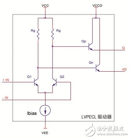
Figure 1. Equivalent circuit diagram of open emitter LVPECL driver
Standard terminalFigure 2 shows a standard DC-coupled LVPECL terminal. The driver output current is set by the external Zo resistor and the VTT terminal voltage. Since the VTT termination voltage is generated by the -2V regulator of Vcco, the output driver current is not affected by the Vcco variable. The main drawback is the need for a regulator, although it does maintain the emitter current of the driver in the first order, regardless of Vcco variations.
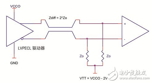
Figure 2. Standard LVPECL Terminal
Thévenin equivalent terminalThe alternative Thévenin equivalent termination shown in Figure 3 to provide 3.3V and 2.5V currents uses two resistor strings to generate the VTT voltage, so that the regulator can no longer be used, but it has its drawbacks.
1) The R1 and R2 bias resistor strings in Figure 3 require significant power loss to generate the Thévenin voltage. The power loss depends on the high output voltage (Voh) and low output voltage (Vol) of a particular driver; see the “Case Study†section below.
2) The Vcco rate of change is fed forward through the bias voltage divider to the Thévenin equivalent VTT voltage; 39% means Vcco = 3.3V and 20% means Vcco = 2.5V. Therefore, the VTT voltage is only limited to the nominal Vcco. The control of the emitter current is not as effective as the standard VTT=VCC-2.0V terminal.
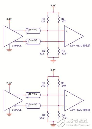
Figure 3, 3.3V and 2.5V Thévenin Equivalent LVPECL Termination
T terminalThe T resistor network shown in Figure 4 solves many of the deficiencies of Thévenin terminals. The common-mode voltage across the RTT is called VTT, which is equivalent to VTT = Vcco-2.0V. Keep in mind that the specific VTT voltage is not a design standard; the LVPECL receiver never detects VTT but detects the emitter voltage. VTT is only important for standard terminals because VTT feeds the VCCO to the terminal to control the emitter current. In contrast, the T-terminal exerts control over the emitter current through negative feedback. Figure 4 The VTT voltage in an LVPECL T-Terminal network indirectly depends on the Voh and Vol levels of a particular LVPECL driver and the minimum emitter current the designer chooses for a logic-0 driver output.
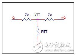
Figure 4. LVPECL T Termination Network
1) The T terminal is powered directly from the driver supply, thus eliminating the functional loss of the Thévenin bias string.
2) The rate of change in Vcco returned to the T-network VTT voltage through the common-mode impedance is greater than the rate of change returned through the Thévenin network, thus allowing better control of the emitter current. See the "Emitter Current Control" section below for details.
3) The common mode impedance can be adjusted and the negative feedback can be adjusted to stabilize the driver current for changes in Voh and Vol due to variations in Vcco, temperature, and device handling.
PI terminalYou can use the famous resistor network star-triangle relationship to generate equivalent PI termination from the T terminal. Figure 5 below shows the element values ​​of a PI network scaled by the T network.
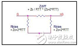
Figure 5, PI terminal network
Rarely used PI terminals have a layout advantage over T terminals; it can be safely placed on top. The common mode impedance of T must pass through layers other than the top layer.
Emitter current controlT-terminals provide better emitter current control than Thévenin terminals. The Thévenin terminal stabilizes the current by feeding forward the VTT voltage to the terminal to feed the Vcco rate of change α. In contrast, the T-terminal uses negative feedback by detecting the emitter current across the emitter resistor and can only be used as a single emitter follower.
Each variation of Vcco can be constructed for each terminal as shown in Figure 6 to illustrate this change in performance. For each terminal, the circuit starts with Vcco, passes through the base-emitter junction Rg of the corresponding output transistor, and then passes through the terminal where Rg is switched into the emitter current path. For simplicity, the base extension resistor has been incorporated into the gain setting resistor Rg. Due to the two bias strings, Thévenin Icco is half the total current.
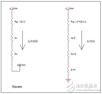
Figure 6. Thévenin and T-Terminal Emitter Current Control Circuits
The transfer function for each circuit can be written immediately from Figure 8. In each transfer function, the reterm has been deprecated; it is relatively small compared to Rg and Zo. In addition, the small size of re means that the equivalent half-circuit of the logic 1 transistor and the logic 0 transistor of the T-terminal is the same.
Since the values ​​of Rg and β depend on the internal design and processing of a particular LVPECL driver, the following "case study" chapter is expected. When VCCO = 3.3V and RTT = 77 ohms, the two transfer functions are relative to each other in Figure 8 below. Designed for Rg/(β+1).
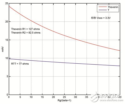
Figure 7. Thévenin and T terminal variations in emitter currents to accommodate Vcco variations
For example, if Rg/(β+1) = 0, the β value is large and the Rg value is small (Ibias in Figure 1 is high). In this limited condition, the transfer function depends only on the external resistor. More practically, if Ibias = 0.5 mA, Rg = 1.6 kohms, and β = 100, then Rg/(β+1) ≈16.
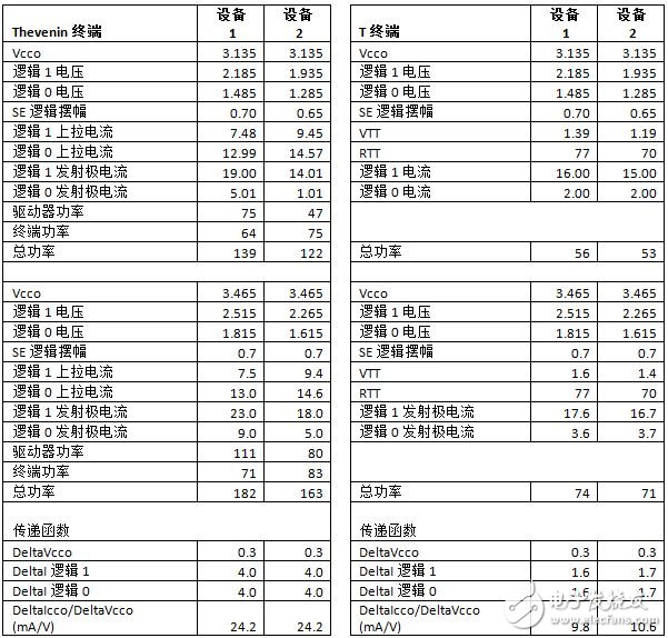
case studyUnder the ±5% Vcco condition, two different LVPECL drivers with different Voh and Vol values ​​were compared to the industry for each terminal. The T-terminal will be optimized for each device and designed to have a logic 0 emitter current of at least 2 mA when Vcco is -5% to achieve the best balance between switching speed and power. For each case, the spreadsheet values ​​are calculated using KVL and KCL. For comprehensive accounting, the power of the drivers and terminals in each case was calculated.
As shown in Figure 1 below, because the RTT of the T-terminal can be freely selected, it has the design flexibility to reduce the total driver current while still ensuring the lowest logic 0 emitter current. The fixed resistance value of Thévenin terminals is not. Please note that there is a large fluctuation in the emitter current of logic 0 on the Vcco of the fixed device Thévenin terminal and on the device. If the changes brought about by the equipment processing and temperature are also taken into account, the difference between the two terminals will become even greater.
All currents and voltages are calculated using the typical Voh and Vol values ​​in the 3.3V power supply datasheet. As there is no other description in this data sheet, Voh and Vol assume a 1:1 variation with Vcco. Therefore, these cases are equivalent to setting Rg/(β+1) =0. The current is in mA and the power is in mW units.
Table 1, Comparison of Two Different Drivers for Thévenin and T-Terminals
In an era when integrated circuit technology is far from effective, LVPECL is available as a high-speed input-output standard. The LVPECL driver must finally use external passive components to be satisfactory, but it must be designed to complement the driver's output logic levels Voh and Vol. As we all know, existing terminal networks have disadvantages. Using Pi or T resistor networks can overcome these shortcomings and enable more adaptable, more energy-efficient designs.
Copper Dryer Filter
copper filter driers are designed to absorb moisture, acid, and to filter out impurities. Normally be installed as component and replaced as repair part for both domestic and commercial refrigerators, freezers.
This fliter is for air conditioner water tank or fridge, replacing your broken or old one.
Used in two-way circulation refrigeration system tubes
Absorb moisture and acidic harmful substances in the refrigeration system and filter impurities.
This filter dryer is fit for refrigerators (but refrigerator is not including here)
Copper Dryer Filter,Refrigeration Dryer Filter,Refrigerator Water Dryer Filter,Refrigerator Copper Filter Drier
FOSHAN SHUNDE JUNSHENG ELECTRICAL APPLIANCES CO.,LTD. , https://www.junshengcondenser.com