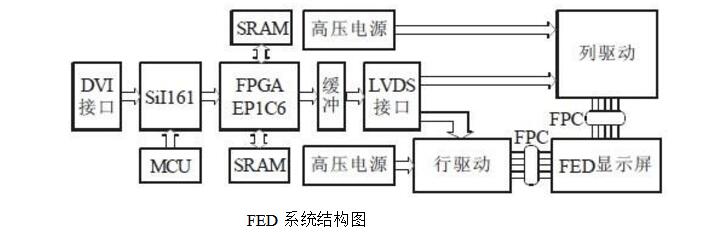
FED --- FieldEmissionDisplay (or Field Effect Display) refers to the so-called electron emission refers to the process of electrons escaping from the cathode into a vacuum or other gaseous medium. All objects contain a large amount of electrons. Under normal conditions, they do not escape. When the electrons get enough energy to overcome the force that prevents them from escaping the surface of the object, electron emission occurs.

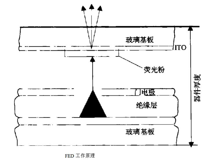
Field electron emission, also known as cold electron emission, is simply summarized as the addition of a strong electric field on the surface of the cathode. In addition, no additional energy is required. The electrons in the cathode have sufficient energy to escape from the surface and form electrons. emission. One of its important applications is the field emission display (FED). The principle is that the strong electric field forces the electrons to release from the tip of the cathode material. The electrons accelerate the anodic electric field, bombard the phosphor on the screen, excite the phosphor and emit light, and there are tens of thousands of tiny points behind each phosphor point. The electron emitters, FED rely on field emission technology to achieve the electron emission source, do not use thermal energy, instead of the hot electron gun in the CRT picture tube, the field emission electron beam energy distribution range is narrower than the traditional hot electron beam and has a high brightness, available This technology enables the design and production of flat panel displays.

FED display technology has the advantages of high luminous efficiency, fast dynamic response, and good color. It does not require auxiliary devices such as backlight source, filter film, polarizer, or other optical films. Therefore, the structure of FED is simpler than LCD, and the response speed is faster. Larger, the ambient temperature is not as strict as the LCD. The advantages are as follows: 1) The power consumption of the backlight module can be reduced, and a high contrast ratio of more than 20000:1 can be achieved. 2) FED utilizes the self-luminous nature of fluorescent powders, wide viewing angles, and high color quality at large viewing angles. 3) Operating temperature range, high environmental resistance. 4) High color purity and color reproducibility can be exhibited. 5) The heating power consumption of the thermal emission can be saved, so the power consumption is low and the luminous efficiency is high.
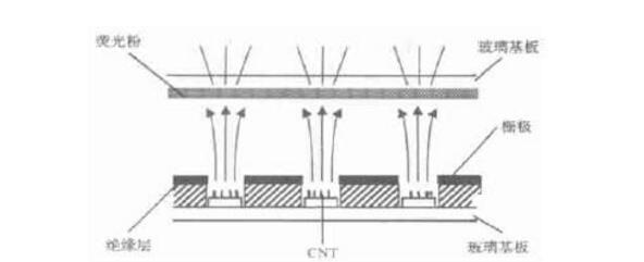
The form of field emission of FED electrons can be broadly divided into the following three types: tip external field electron emission; dielectric film (media coating) internal field electron emission; carbon nanotube field induced electron emission.
FED display device manufacturing processThe basic structure of the FED display panel is shown in Figure 1. In a triode FED, the electric field generated by the gate voltage determines the strength of the cathode electron emission. The uniformity is mainly affected by the following factors (directly affecting the image quality and resolution): cathode and The spacing between the grids, the diameter of the grid holes, the cathode material, etc., the uniform production of phosphors.

Fig. 1 Schematic diagram of a triode FED
The fabrication node of the FED display device lies in the matching and sophisticatedness of the cathode plate and the phosphor plate. The process flow of the cathode plate is: cathode electrode→media layer→gate electrode→rotary fabrication transition layer→microcone tip production (difficulties). The process flow of the phosphor plate is: black bar→phosphor powder.
The ideal field emission device has the following structure:
(1) Very fine micro-cone tips; (2) Cathode materials have a low work function that favors electron emission; (3) Cathode materials have a high melting point that withstands high temperatures; (4) Small gate openings facilitate the increase of electric field strength. (5) The dense dielectric layer prevents leakage or breakdown between the electrodes.
1, FED cathode board productionThe FED cathode plate production includes the selection and cleaning process of the substrate glass, the electrode manufacturing process on the cathode plate, the coating process, and the cathode manufacturing process.
(1) Nano-Spindt, whose structure is prepared using a novel technology (based on thin-film technology and semiconductor micromachining technology), using coating and etching; (2) substrate, carrying film and slurry Material and insulation from the air. Therefore, it is required to be smooth and have a certain strength, and to cope with thermal expansion and withstand a certain pressure. Usually, high-knife glass is selected. (3) The configuration of the spacers and the positions on the two substrates need to be optimized to prevent deformation of the display panel; (4) ) Vent to extract air from the screen.
The electrode manufacturing process includes coating, printing, and etching. The coating process includes a metallized film and an insulating film.
2, FED anode plate productionThe phosphor plate is composed of a substrate, an anode, and a phosphor layer and can generate visible light. The phosphor plate uses the same substrate as the cathode plate. The phosphor used in the FED is of the electron excitation type, and the distance between the gate and the anode is as short as possible to focus. Since the anode voltage is high (up to tens of thousands of volts), the distance between the anode and the gate is large enough to avoid breakdown.
(1) Black strip: black material is vapor-deposited, and a black stripe is formed by using a photolithography process to increase the contrast and define phosphors to be mixed with each other; (2) R, G, and B phosphors: printed with photosensitivity respectively A certain color phosphor slurry, and then exposure (non-contact) development, remove the phosphor powder on the other two color powder position; (3) anode: a layer of metal Cr deposited on the phosphor layer, and then evaporated A layer of C, and finally deposited a layer of aluminum film to form an anode, the electrode is drawn using a common electrode.
3, FED separator (support column) productionThe separator mainly ensures uniform spacing between the two plates of the cathode plate and the phosphor plate, and functions as a support and isolation. Generally, the separator is a ceramic material whose height determines the distance between the grid and the anode. FED is a high-vacuum device in which the spacer supports the substrate to prevent the atmospheric pressure from deforming or breaking the substrate. Therefore, the spacer material must meet the requirements of high vacuum and compression resistance. The width of the spacer is only tens of micrometers. Since the spacer cannot emit light, the width of the spacer is also reduced. The height of the spacer is usually as small as um. The higher the anode pressure, the higher the spacer height, and the brightness of the display. The efficiency also increases; hundreds of volts - tens of thousands of volts of positive pressure require 100um - 1000um of the insulator can meet the requirements of the grid Yang is not broken down, and the high grid spacing will cause the electron beam to spread out, bombardment to The electronic spot of the phosphor also increases accordingly. The spacer must have a high ratio of height to width. The general production process is screen printing and sandblasting.
4. Sealing and degassing process of FED displayThe main process flow is: degassing → sealing frame production → glass punching → pairing → sealing → vacuuming → baking and eliminating gas. On the cathode glass substrate, the exhaust pipe is connected first, and the insulator is placed on the cathode emission surface, and the row spacing must conform to a certain placement rule. A glass paste with a low melting point is coated on the four peripheral surfaces of the mating cathode and anode substrate glass, and the electrode lead is left, and the two substrate glasses are subjected to a drying process as a whole, and then the sealing is performed. Heat sealed in the room. Next, vacuum is applied to the sealing screen to perform suction and sealing; in order to ensure the stability of the cathode electron emission in the screen, the sealing condition is usually a vacuum of 1×10⁻⁴ Pa, and then the gas is roasted and eliminated to complete the entire process. Degassing process.
5. Test and Experience of FED DisplaySimilar to the production of PDP screens, sealed FED screens must also undergo testing and aging processes, which is also the last step of the general screen-making process. The test refers to placing the sealed screen on the test fixture and turning on the test circuit to see its overall performance. Generally, it will also input several test signals to see whether the screen shows the ideal image, and then according to the test results. The relevant process of the screen is adjusted and improved. The old refinery is to remove the degassed FED display and perform the necessary electrical treatment to achieve the standard. Its role is to fully activate the cathode, stabilize the emission, further degas the in-panel electrodes, and increase the dielectric strength between the electrodes to achieve stable FED. Electrical and high frequency performance.
Remote Monitor Systems Battery
Remote Monitor Systems Battery,E Cigarette Lithium Battery,Semi Tight Lithium Battery,Intelligent Oem Lithium Battery
Jiangmen Hongli Energy Co.ltd , https://www.honglienergy.com