For many years, semiconductor manufacturers engaged in power management business have tried to keep up with the needs of end-system users. More and more portable electronic products are functionally refurbished. These products require peak performance and require designers to achieve the highest possible efficiency within the physical dimensions of the device. While the battery industry is working hard to develop alternative battery technologies that have higher power than traditional nickel-cadmium (NiCd) batteries, it is far from meeting the energy needs of next-generation portable devices. As a result, portable applications have to seek innovative development in low-power circuit design, enabling design engineers to use end-use systems with the highest possible efficiency. In portable devices, components are a major part of the power budget, and it is clear that to keep up with demand changes, semiconductor device manufacturers need to innovate to help reduce the power consumption of portable products.
Taking mobile phones as an example, reducing the operating voltage of the main components in handheld devices such as analog and digital baseband chips is one of the ways to reduce power consumption. When the DSP or microprocessor is not required for maximum performance, the core supply voltage can be reduced and the clock frequency reduced. More and more new generation low-power applications use this technology to save as much system power as possible. The formula PC~(VC)2.F describes the power consumption of a DSP core. Here, PC is the power consumption of the core, VC is the core voltage, and F is the core clock frequency. Reducing the internal clock frequency reduces power consumption, and lowering the core supply voltage can reduce power consumption even more.
What can advanced silicon and packaging technologies do?
There are many design factors for the performance of emerging high-power portable devices. This article will focus on the most common power switching power MOSFETs in low-voltage applications, illustrating the impact of the latest silicon technology breakthroughs on increasing power requirements. To illustrate the impact of these technological advances, it is necessary to understand some of the key parameters of power MOSFETs.
The on-resistance (rDS(on)) of the channel is controlled by the lateral and longitudinal electric fields of the channel. The channel resistance is mainly determined by the gate-to-source voltage difference. When VGS exceeds the threshold voltage (VGS(th)), the FET begins to conduct. Many operations require a switch ground point. The resistance of the power MOSFET channel is related to the physical size determined by the formula R = L / A, where ï² is the resistivity, L is the channel length, and A is W x T, which is the cross-sectional area of ​​the channel.
In a typical FET structure, L and W are determined by the geometry of the device, and the channel thickness T is the distance between the two depletion layers. The position of the depletion layer varies with the gate-source bias voltage or the drain-source voltage. The position of the depletion layer varies with the gate-source bias voltage or the drain-source voltage. When T is reduced to zero under the influence of VGS and VDS, the two opposite-side depletion layers are connected together, and the increased channel resistance (rDS(on)) approaches infinity.
Figure 1 is a plot of rDS(on) versus VGS characteristics. Region 1 corresponds to the case where the accumulated charge is insufficient to cause a reverse. The corresponding condition for region 2 is that there is sufficient charge to reverse a portion of the P region and form a channel, but this is not enough because the "space charge" effect is also important. Region 3 corresponds to a case where the charge is limited, and when the gate potential is raised, rDS(on) does not change significantly.
Figure 1: Relationship between rDS(on) and VGS characteristics
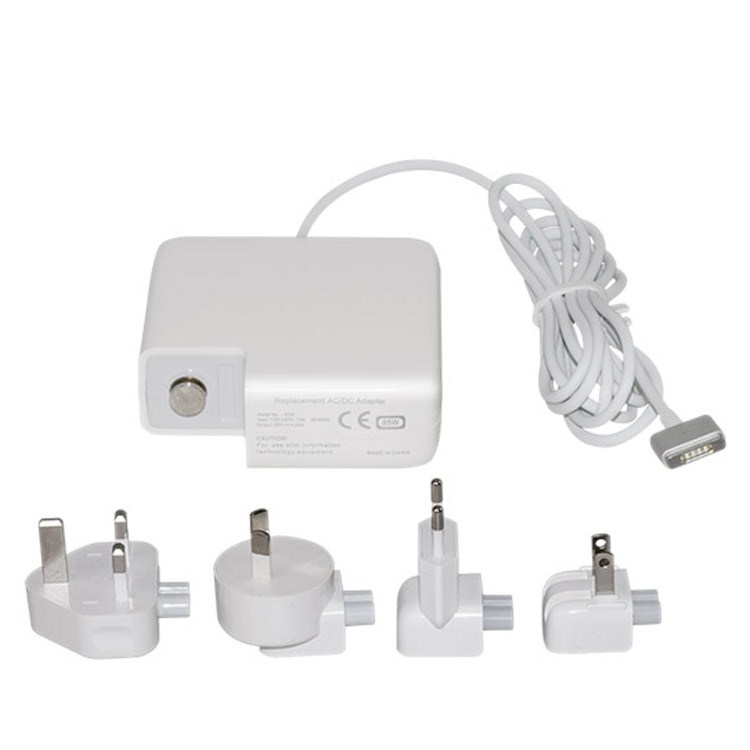
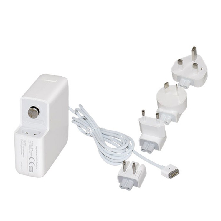
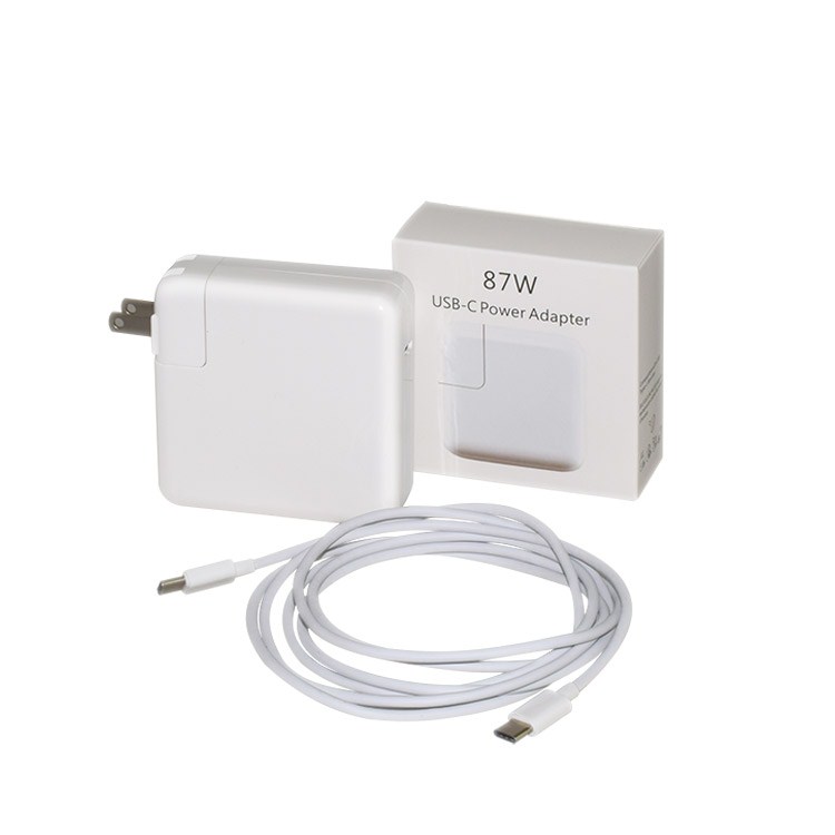
Whether you have an Apple Ibook, an Apple Powerbook or indeed an Apple Macbook Air, we will have the Apple Laptop Charger suitable for your Apple laptop. Apple is a high quality brand, and therefore Apple laptop charger must be high quality too.
Apple laptop charger include apple macbook pro charger series and apple macbook air charger series. Yidashun not only can offer 45W 60W 85W old mac charger with magsafe 1.0 and 2.0 tip, but also can offer new 29W 30W 61W 87W USB C power Adapter. And also we can silkprint your logo on the chargers, and also can customize the color package.
If you want to look for a factory which can produce range models of the macbook charger, and also with high quality, contact Yidashun , we can offer you all kinds of replacement apple adapter. and also support you high quality with 2 years' warranty.
Yidahsun's laptop adapter is with smart IC to protect your laptop with over current protection, over load protection, short circuit protection, over heat protection. All our mac laptop charger is Brand New Replacement Product, works as Genuine parts, 100% OEM Compatible!


Apple Laptop Charger,Apple Computer Charger,Apple Macbook Charger,Mac Laptop Charger
Shenzhen Yidashun Technology Co., Ltd. , https://www.ydsadapter.com