Under the control of the selected variable, a certain road data is selected from the multiple input data and sent to the output end. For a multiplexer with 2n inputs and 1 output, there are n selectable variables.
2 typical chipsA typical mid-range multiplexer has a dual 4-way data selector 74153. Its pinout diagram and logic symbols are shown in Figures 1 (a) and (b).
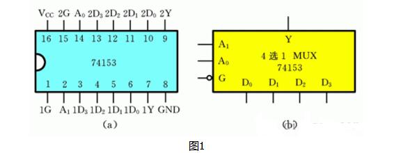
The data selector 74153 includes two 4-way data selectors. Each selector receives four data inputs and generates one output. The two 4-way data selectors share two selection variables. The chip has 16 leads, of which 1D0 to 1D3 and 2D0 to 2D3 are 8 data input lines, A1 and A0 are the selected input lines, 1Y and 2Y are the 2 output lines, 1G and 2G are the enable control terminals, and 1 is the other. Power cord and 1 ground wire.
The output function expression of the 4-way data selector is

In the formula, mi is the smallest item that constitutes a selection variable.
3 applicationsIn addition to completing the basic functions of selecting multiple channels of data, the multiplexer can also be used to implement parallel-to-serial conversion of data, generation of sequence signals, and implementation of various logic function functions.
For example, a 4-way selector 74153 is used to implement the following logic function

The solution given function is a 3-variable function. Since the 4-way selector has 2 selection control variables, when it is used to implement the 3-variable function function, it should first select 2 control variables from the 3 variables of the function as the selection control variable. Then determine the selector's data input. Assuming that A and B are connected to the selection control terminals A1 and A0, the expression of the function F can be expressed as follows:

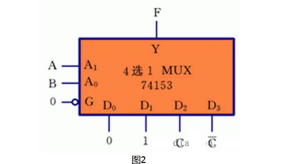
Obviously, to make the output Y of the 4-way selector equal to the function F, only:. Based on this, the logic circuit can be drawn as shown in Figure 2. Similarly, you can also choose A, C, or B, C as the selection control variables, select different control variables, and different data inputs.
design background:
The design is based on digital electronic technology, and the data is selected from the four-digit data according to the input signal to achieve the desired logic function.
Design:
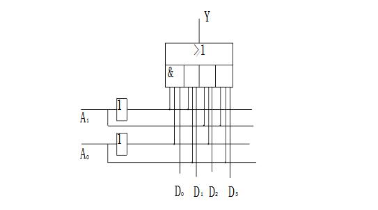
DIP switch is used for four-bit data and input of two control terminals. LED is used for output. Different combinations of control input terminals s1 and s0 are formed by dialing switches, and the relationship between LED and data input terminals a, b, c, d is observed. Selecting the correctness of a data selector design. Using a combination of logic gates AND, OR, and NOT to express a 4-to-1 data selector, the output signal value is controlled by controlling the input signal.
Its logic circuit is as follows:
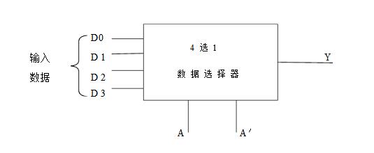
Its schematic block diagram is as follows:
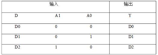
Among them input data port is DO, D1, D2, D3, A, A is the control signal, Y is the output.
When AA' = "OO", output Y = D0;
When AA' = "01", output Y = D1;
When AA' = "10", output Y = D2;
When AA' = "11", the output Y = D3;
The truth table is as follows:

(1) Design Ideas
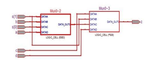
When designing a multiplexer of four selectors, the input s is defined as the standard. The data type of the signal Z output as SIDLOGIC is defined as the 2-bit standard logic vector bit STD_LOGIC_VECTOR (1DOWNTO0). Use the LBRATY statement and the USE statement to open the IEEE library package STDLOGIC_1164.ALL. When the signal is input, the program selects the output according to the input command. For example, when the input signal is “OOâ€, the value of a is given to z, and then the value of z is output, the input signal is “11â€, and the value of a is given to z. , and then output the value of z. If the input signal is a value other than the already defined four signals (ie, when the positive conditional statement is not satisfied), the output value is x, and the value of x is given to the output signal Z. In this way, four data selection functions can be selected.
program
LIBRARY positive EE:
USE
IEEE.STD_LOGIC_1164.ALL:
ENTITYmux41is
PORT(a,bcd:NSTD_LOGIC:
INSTD_LOGIC_VECTOR (1
DOWNTO0):
STD_LOGIC):
OUT
END
Mux41:
IS
ARCHITECTUREoneOF
Mux41
BEGIN
PROCESS(s,abcd)
BEGIN
IS
CASES
WHEN "00" = "z" = a:
WHEN "01" = "z" = b:
WHEN "10" = "z" = c:
WHEN "11" = "z" = d:
WHENOTHERS=â€z†-=null:
END
CASE;
ENDPROCESS:
END
One;
operation result
When the signal "OO" is input, the output signal z has a value of 'a':
When the input signal "01", the output signal z is 'b';
When the signal "10" is input, the value of the output signal z is 'c':
When the signal "11" is input, the value of the output signal z is 'd':
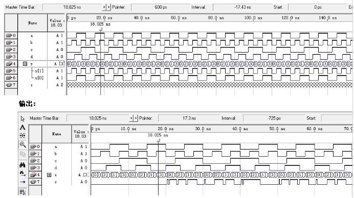
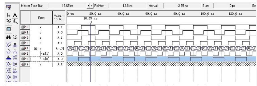
Waveform simulation and description
enter:
The waveform period is 10ns, the waveform period of b is 5ns, the waveform period of c is 15ns, and the waveform period of d is 8nsos [1] The waveform period is 5ns. The waveform period is 10ns.
(2) Design Ideas
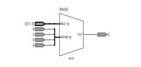
Defining six input signals, one output signal, when the control signal A = '1', the value of muxval increases by one, that is, muxval = muxva1+1 When the control signal B = '1', the value of muxval increases by two, that is, muxval- Muxval+2. When the input value is 'i0', the value of output q is 0. When the input value is "i1', the value of output q is 1, when the input value is 'i2', the value of output q is 2, when When the input value is 'i3', the value of output q is 3.
program
USE is EE.STD LOGIC 1164.ALL;
ENTITY mus41
IS
(i0ji1,i2,i3,a,b :N STD_LOGIC;
PORT
:OUT
STD_LOGIC );
ENS mux4;
OF
Mux4 IS
ARCH ITE CT URE b_mux4
BE GN
Process (i0,il,i2,i3,a,)
Variable
0;
Downto
Musval
:integer rang
Begin
m uxv al :=0;
If (a='l')
Musval:muxval+ l; end if;
Then
If (b='I') then
Muxval :muxwal + 2; end
If;
Is
Muxval
Case
w hen 0= †q “= i0;
When l= †q “= il;
When2="q"=2;
When3="q"=i3;
Others= 》null;
When
End
Ca se;
End process;
END b_mux4;
operation result
When the signal "OO" is input, the value of the output signal z is 'i0':
When the signal "01" is input, the value of the output signal z is 'i1':
When the signal "10" is input, the value of the output signal z is 'i2':
When the signal "11" is input, the value of the output signal z is 'i3';
Waveform simulation and description
The waveform period of a is 20ns, the waveform period of b is 15ns, the waveform period of c is 20ns, the waveform period of d is 15ns, the waveform period of s is 8ns, and the waveform period of s is 16ns.
Output
TAIZHOU HUADONG INSULATED MATERIAL CO.,LTD , https://www.thim-insulator.com