Switching power supplies have extremely high value due to their small size, low cost, and high efficiency.
However, its biggest drawback is the high output noise caused by high switching transients. This shortcoming makes them impossible to use in high-performance analog circuits based on linear regulators.
However, it turns out that in many applications, a properly filtered switching converter can replace a linear regulator to generate a low noise power supply.
Therefore, it is necessary to design a multi-stage filter that is optimized and damped to eliminate the output noise of the switching power converter.
The example circuit in this article will use a boost converter, but the result can be directly applied to any DC-DC converter. Figure 1 shows the basic waveform of the boost converter in constant current mode (CCM).

Figure 1. Basic voltage and current waveforms of a boost converter
The importance of the output filter to the boost topology or any other topology with discontinuous current mode is due to its rapid rise and fall times in the current in switch B. This can lead to parasitic inductance in the driver switch, layout, and output capacitor. As a result, in actual use, the output waveform looks more like Figure 2 than Figure 1, even with good layout and use of ceramic output capacitors.
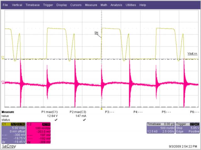
Figure 2. Typical Measurement Waveform of Boost Converter in DCM
The switching ripple (switching frequency) due to the change in capacitive charge is very small compared to the undamped ringing of the output switch, hereinafter referred to as output noise. In general, this output noise range is from 10 MHz to over 100 MHz, far beyond the self-resonant frequency of most ceramic output capacitors. Therefore, adding additional capacitance has little effect on noise attenuation.
There are many different kinds of filters that are suitable for filtering this output. We will explain each filter and give each step of the design.
The formulas in the article are not rigorous and some reasonable assumptions have been made to simplify them to some extent. Some iterations still need to be done because each element affects the values ​​of other elements.
The ADIsimPower design tool avoids this problem by using linearization formulas for component values ​​(such as cost or size) to optimize before actually selecting components, and then optimizing the output after selecting actual components from a database of tens of thousands of devices. . But at the beginning of design, this degree of complexity is not necessary. Using the calculation formula provided, using the SIMPLIS simulator - such as the free ADIsimPETM - or spending some time on a lab bench, you can get a satisfactory design with minimal effort.
Before we start designing the filter, let us first consider what a single-stage filter RC or LC filter can do.
A secondary filter is usually used to reasonably suppress the ripple to a few hundred μV pp and suppress the switching noise to less than 1 mV pp. The buck converter is less noisy because the supply inductance provides good filtering capability. These limitations are because, once the ripple is reduced to the μV level, the noise coupling between the element parasitics and the filter stage begins to become the limiting factor. If you use a lower-noise power supply, add a three-stage filter. However, the reference voltage source of the switching power supply is generally not the lowest noise component and is often affected by jitter noise. These all lead to low-frequency noise (1 Hz to 100 kHz), which is usually not easily filtered. Therefore, for very low noise power supplies, using a single secondary filter and then adding an LDO at the output may be more appropriate.
Before describing the design steps of various types of filters in more detail, the numerical values ​​of various types of filters used in the design steps are defined as follows:
ΔIPP: Approximate peak-to-peak current into the output filter (for ease of calculation, assume a sinusoidal signal. The value depends on the topology. For buck converters, it is the peak-to-peak current in the inductor. For boost converters It is the peak current in switch B (usually a diode).)
ΔVRIPOUT : Output Voltage Ripple Approximation at Converter Switching Frequency
RESR: ESR of the selected output capacitor
FSW : Converter Switching Frequency
CRIP: In the calculation of the output capacitance, it is assumed that all ΔIPPs flow in
ΔVTRANOUT: VOUT changes when ISTEP is applied to the output
ISTEP: Instantaneous change of output load
TSTEP: Approximate response time of the converter to transient changes in the output load
Fu: The crossover frequency of the converter (usually FSW â„10 for buck converters; RHPZ for boost or buck/boost converters) 1/3 position.)
The simplest type of filter is an RC filter, as shown in Figure 3 based on the output of the low-current ADP161x boost design. This filter has the advantage of low cost and does not require damping. However, due to power consumption, it is only useful for very low output current converters. This article assumes that the ceramic capacitor has a lower ESR.
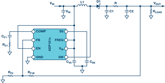
Figure 3. ADP161x Low Output Current Boost Converter Design with an RC Filter at Output
RC Secondary Output Filter Design Procedure
step 1
C1 is selected based on the following conditions: It is assumed that the output ripple approximation of C1 can ignore the remaining filters; 5 mV pp to 20 mV pp is a good choice. C1 can then be calculated by Equation 1.
Step 2
R can be selected based on power consumption. R must be much larger than RESR, capacitor and this filter can work. This limits the output current to less than 50 mA.
Step 3
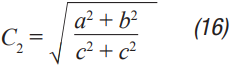
C2 can then be calculated from Equation 2 to Equation 6. A, a, b, and c are intermediate values ​​for simplified calculations and have no practical significance. These formulae assume R < />LOAD and the ESR of each capacitor is small. These are all good assumptions and the introduced errors are small. C2 should be equal to or greater than C1. The ripple in step 1 can be adjusted to make it possible.

 |
 |
 |
For higher current supplies, it is advantageous to replace the resistance in the pi filter with an inductor as in Figure 4. This configuration provides excellent ripple and switching noise rejection and lower power consumption. The problem is that we have now introduced an additional energy storage circuit that may generate resonances. This can cause oscillations and make the power supply unstable. Therefore, the first step in designing this filter is how to select the damping filter. Figure 4 shows three possible damping techniques.

Figure 4. ADP1621 using an output filter and highlighting a variety of different damping techniques
Damping Technique 1: Adding RFILT has the added advantage of less cost and size increase. Damping resistors usually have little or no loss, even in the case of large power supplies. The disadvantage is that it reduces the shunt impedance of the inductor, which greatly reduces the effectiveness of the filter.
Damping technique 2: The advantage of the second technique is that the filter performance is maximized. If an all-ceramic design is desired, the RD can be a discrete resistor in series with the ceramic capacitor. Otherwise, use capacitors with high ESR and large physical size. This extra capacitance (CD) dramatically increases the cost and size of the design.
Damping technique 3: It looks like a great advantage because the damping capacitor CE is added to the output, which may help with transient response and output ripple performance. However, this technique is the most expensive because of the large number of required capacitors.
In addition, the relatively large amount of capacitance at the output reduces the filter's resonant frequency, which in turn reduces the converter's achievable bandwidth - so the third technique is not recommended. For ADIsimPower design tools, we use the first technology because it is less expensive and relatively easy to implement in the automated design steps.
Another issue that needs attention is compensation. Although this may not be intuitive, it is always better to place the filter inside the feedback loop. This is because placing it in the feedback loop helps to suppress the filter to a certain extent, eliminating the DC load offset and the series resistance of the filter while providing better transient response and lower ringing. . Figure 5 shows a Bode plot of a boost converter that adds an LC filter output at the output.
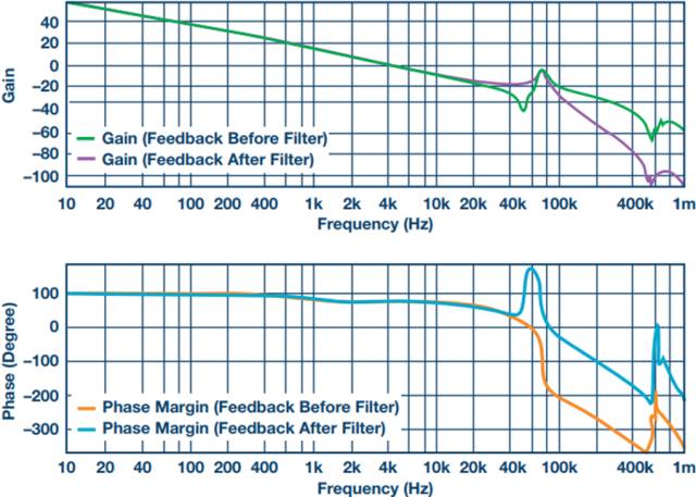
Figure 5. Boost converter with LC filter at the output
Feedback is taken before or after the filter inductance. What people did not think of is that even if the filter is not inside the feedback loop, the open-loop Bode plot still has a very big change. Since the control loop is affected regardless of whether the filter is in the feedback loop, it should also be properly compensated. In general, this means that the target crossover frequency is adjusted down to no more than one-fifth and one-tenth of the filter resonant frequency (FRES).

The design steps of this type of filter are essentially an iterative process because the choice of each element affects the selection of other elements.
LC filter design step using parallel damping resistors (first technique in Figure 4)
step 1
Select C1 so that it is equal to the output filter when there is no output filter. 5 mV to 20 mV pp is a good start. C1 can then be calculated by Equation 8.

Step 2
Select the inductor LFILT. As a rule of thumb, the preferred range is 0.5 μF to 2.2 μF. The inductance should be chosen in accordance with the high self-resonant frequency (SRF). Larger inductors have larger SRFs, which means that their high-frequency noise filtering efficiency is poor. Smaller inductors have less impact on ripple and require more capacitance. The higher the switching frequency, the smaller the inductance. When comparing two inductors with the same inductance value, the device with higher SRF has lower inter-winding capacitance. Inter-winding capacitance acts as a short circuit around the filter, acting on high-frequency noise.
Step 3
As mentioned earlier, adding a filter affects the converter compensation, in particular by reducing the achievable crossover frequency (Fu). According to the calculation of Formula 7, the maximum Fu that can be achieved for the current mode conversion is 1/10 or less of the switching frequency, or 1/5 or less of the filter FRES. Fortunately, most analog loads do not require too high transient response. Equation 9 calculates the required output capacitor approximation (CBW) for the converter output to provide the specified transient current step.
Step 4
Set C2 to the minimum of CBW and C1.
Step 5
Use Equation 10 and Equation 11 to calculate the damping filter resistance approximation. These formulas are not absolutely accurate, but they are the closest closed solutions that do not use generic algebra. The ADIsimPower design tool calculates the RFILT by calculating the open-loop transfer function (OLTF) of the converter when the filter and inductor are short-circuited. The RFILT value is a guess until the filter is only 10 dB above the converter OLTF and the peak of the converter OLTF (inductor short circuit). This technique can be used in simulators such as ADIsimPE or in laboratories using spectrum analyzers.
Step 6
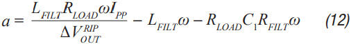
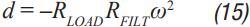
C2 can now be calculated from Equation 12 to Equation 15. a, b, c, and d simplify Formula 16.

 |
 |
Step 7
Steps 3 through 5 should be repeated until an excellent damping filter design that satisfies the required ripple and transient specifications is calculated. It should be noted that these formulas ignore the DC series resistance RDCR of the filter inductance. For lower supply currents, this resistance can be very large. It improves the filter performance by helping to suppress the filter, increasing the required RFILT and also increasing the filter impedance. Both of these effects will greatly improve the filter performance. Therefore, it is cost-effective to trade a small amount of power in LFILT for low noise performance, which improves noise performance. The core loss in LFILT also helps to attenuate some of the high frequency noise. Therefore, a high current-powered ferromagnetic core is a good choice. They have smaller dimensions and lower costs with the same current capability. Of course, ADIsimPower has the filter inductor resistance value and the ESR value of the two capacitors to achieve the highest accuracy.
Step 8
When selecting the actual component to match the calculated value, note that any ceramic capacitor needs to be derated to handle the DC bias.
As mentioned earlier, Figure 4 shows two possible techniques for suppressing filters. If no shunt resistance is selected, the CD can be selected to suppress the filter. This adds some cost, but it provides the best filter performance compared to any other technology.
LC filter design step using RC damping network (2nd technology in Fig. 4)
step 1
As in the previous topology, select C1 to make it equal to when there is no output filter. 10 mV pp to 100 mV pp is a good start, depending on the final target output ripple. C1 can then be calculated by Equation 8. C1 can use smaller values ​​than the previous topology in this topology because the filter is more efficient.
Step 2
In the previous topology, choose an inductor with a value of 0.5 μH to 2.2 μH. For a converter from 500 kHz to 1200 kHz, 1 μH is a good value.
Step 3
As before, C2 can be selected from Equation 16, but RFILT should be set to a larger value, such as 1 MΩ, because the component will not be installed. Whether or not C1 has additional capacitance, the reason that its value does not change is that in order to provide good damping, RD will be large enough that the CD will not drastically reduce the ripple. Set C2 to the minimum calculated by C2, CBW, and C1. It is useful to go back to step 1 and adjust the ripple on C1 so that the calculated C2 is approximately equal to CBW and C1.
Step 4
The value of the CD should be equal to C1. In theory, using a larger capacitor can achieve more suppression of the filter, but it unnecessarily increases the cost and size, and will reduce the converter bandwidth.
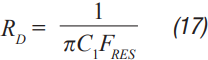
Step 5
RD can be calculated by Equation 17. FRES is calculated by Equation 7, ignoring the CD. This is a good approximation because Rd is usually large enough that the CD hardly affects the filter resonance position.
Step 6
Now that both CD and RD have been calculated, ceramic capacitors with series resistors can be used, or tantalum capacitors with large ESR or similar capacitors can be selected to meet the calculated specifications.
Step 7:
When selecting the actual component to match the calculated value, note that any ceramic capacitor needs to be derated to handle the DC bias.
Another filter technique is to replace the L in the previous filter with ferrite beads. However, this solution has many disadvantages, it limits the effectiveness of switching noise filtering, and there is little benefit to the switching ripple. The first is saturation. The ferrite bead will saturate at a very low bias current level, which means that the ferrite will be much lower than indicated by the zero bias curve in all data sheets. It may still need suppression because it is still an inductor and therefore will follow the output inductor resonance. However, inductors are now a variable and are extremely poorly characterized with very little data that most data sheets can provide. For this reason, the use of ferrite beads as a secondary filter is not recommended, but it can be used downstream to further reduce the extremely high frequency noise.
in conclusion
Above, we provide a variety of switching power supply output filter technologies. This article provides a step-by-step design process for each topology, reducing guessing time and reducing inspection in filter designs. The formulae in this article have been simplified to a certain extent. You can achieve rapid design by understanding how much the secondary output filter can achieve.
Ningbo Autrends International Trade Co.,Ltd. , https://www.supervapebar.com