The plane is parallel incident first, the energy is 400keV. In the material + take r = 0.lcm, h = 48nm and r = 0.lcm, h = 2nm and if there are thousands of small r = 0.lcm, h = 30um Volume grid element as a reference. 2 electron beam irradiation X380n N, P type single crystal silicon wafer, electron irradiation of the sample on a 2MeV linear electron accelerator, the electron energy is 400keV, the beam intensity is 1.67Xl7A.cnf2, the irradiation fluence is 2Xl16cnf2. During irradiation, the beam was scanned laterally to ensure that the sample was irradiated uniformly on the illuminated surface.
EPR test The EPR experiment was conducted on a Japanese ES-FA200 electronic spin resonance spectrometer with a microwave power of 5mW, a modulation frequency of 100kHz, and a temperature of 180k. The analysis samples were 4 N, P types with doping concentrations lxl015cm3, lxl017Cm'3 Monocrystalline silicon wafer. During EPR measurement, the surface of the sample before and after irradiation is perpendicular to the direction of the magnetic field and remains basically the same.
The XPS test analysis sample is two N, P type single crystal silicon wafers with a doping concentration of lxl017cm3. The experimental equipment is XSAM800 X-ray photoelectron spectrometer. The sample is excited by AlKa rays. The sample is first bombarded with Ar- for 5 minutes during the experiment. 2nm surface layer, thus removing impurities adsorbed on the surface.
2 Results and discussion 2.1 The determination of the energy distribution in silicon gives the simulation calculation of the 400keV electron beam irradiating the variation curve of the deposition energy and depth of single-crystal Si with different doping types. It can be seen from the figure that the energy distribution of N-type (P-doped) and intrinsic silicon is almost the same, while P-type (B-doped) silicon has a double peak position, and the energy peak is significantly reduced. From this, we can obtain the 400keV electron beam at a thickness of The energy deposition ratio of 380um silicon wafer oxide layer, interface transition layer and bulk silicon energy is shown in Table 1. Subsequently, the energy deposition-depth curves of P and N doping types with different doping concentrations are obtained respectively. Shown in comparison, it is shown that compared with the doping concentration, the effect of different doping types on electron energy deposition is more obvious, and compared with the N-type, the P-type deposition curve fluctuates as the doping concentration changes.
Table 1 Electron energy deposition in Si-Si02 sample transition surface doped oxide-like layer rotation deposition sample total IK amount deposition layer type intrinsic 400keV electron beam in P, B doped silicon energy deposition-depth curve 400keV electron in a) N-type b) P-type silicon energy deposition-depth curve at different doping concentrations 2.2 Irradiation effect of silicon wafers The EPR spectra of 4 types of samples before and after electron irradiation have been processed accordingly, see. The figure shows that there is an obvious intrinsic defect absorption peak before irradiation, which shows that there is a strong background noise from silicon defects 1121. From the figure, it can be seen that there are mainly four types of P or N type Si Defect types, namely Pb center, P-related center (B-related center), E 'center, P0HC (Branch Oxygen-Hole) center (B0HC (Boron Oxygen-Hole) center), among which Pb center, and P, The intensity of B-related defect centers did not change much before and after irradiation. The E 'center (g = 2.000-2.0010) had a low concentration relative to the POHC (B0HC) center, and its hump was not clearly observed, while the P0HC and B0HC centers For the two types of N and P, there are obvious differences after irradiation. For the P-type boron-oxygen center, the change is not large after irradiation, while the N-type phosphorus-oxygen center has obvious changes after irradiation. In addition, for the same doping type, it can be seen that high doping is also For materials with lower resistivity, the change intensity of defect center after irradiation is stronger than that of materials with low doping resistivity.
EPR spectra before and after electron irradiation. The samples after electron beam irradiation were analyzed by XPS. Compared with the unirradiated samples, the chemical structure of 51312 system has obvious changes. 6 shows P and N type (111) silicon substrates, respectively The change of the Si, B1S, and Pff core energy levels in the upper interface region before and after the 400keV electron beam irradiation shows that the relative content of Sk in the Si ~ -B state of the interface region of the B-doped silicon substrate is slightly improved after electron irradiation. , And the half width of the energy level spectrum peak of the Si2 state is slightly reduced, showing that the silicon transition state component is reduced, while its content is relatively slightly improved, the peak position is 99. 25eV 5 peaks (including B-Si The relative content of the bond peak, whose binding energy is close to that of pure Gui Siff binding energy of 99.45eV), decreases slightly. At the same time, as can be seen from the B1S core energy level spectrum, after irradiation, the relative BIS of the B-Si state The increase in content indicates that the relative content of pure silicon has decreased slightly. In addition, with the weakening of the BB peak strength, the B ~ 0 bond peak has increased, and the half-height width has decreased, which indicates that the boron-oxygen bonding configuration has a tendency to simplify. The above results show that the electron-irradiation of the interface region of the B-doped silicon substrate does not produce a new chemical configuration, and the bonding ability of silicon, boron and oxygen is slightly enhanced. From the core energy level spectrum, it can be seen that the P-Si bond peak intensity in the interface region of the P-doped silicon substrate is significantly weakened after electron irradiation, and the Si2P peak at 99.5eV (including the P-Si bond peak, its binding energy is also The relative content of Gui's Si2P binding energy is close to 99.45eV), which indicates that the pure silicon content is also significantly reduced. At this time, the relative content of the oxidation state increases, the peak half width becomes wider, and the peak position shifts, suggesting that the irradiation increases the chemical configuration of the silicon transition state. The Pa core level spectrum proves this. It can be seen that when the phosphorus impurity state has not changed, and the phosphorus-silicon bonding ability has decreased, the oxidation component has changed significantly. Among them, while the P ~ bond peak is strongly enhanced, the half width increases, and the peak position moves to the high energy direction, which is consistent with the Siff core energy level spectrum. In addition, we see a peak at 133.95eV before the sample is irradiated. After irradiation, the peak intensity jumped sharply, and the half width also decreased sharply. At the same time, the peak position shifted to the low energy direction. Corresponding to the bonding of the binding energy, combined with the EPR test results, it is believed that the peak may be Hole formation. Compared with the former results, the relative content and configuration of each component in the interface region of P-doped silicon substrate changed significantly before and after electron irradiation.
Interface area core level spectrum a) unirradiated, b) 400keV electron irradiation interface area BIS core level spectrum a) unirradiated, b) 400keV electron irradiation Si-Si02 interface on B-doped silicon substrate Electron irradiation XPS spectrum interface area Sk core energy level spectrum a) unirradiated, b) 400keV electron irradiation interface area fV core energy level spectrum a) unirradiated, b) 400keV electron irradiation doped P (111) XPS spectrum of electron irradiation on SiSi02 interface on silicon substrate. 3 Discussion From the energy deposition distribution in Table I, although the total deposition energy of the P-type sample has decreased, the energy deposited in the oxide layer and the interface transition layer accounts for 1.15% of the total deposition energy, compared to the intrinsic sample L08% Compared with the 1.05% of the N-type sample, it can be seen that the low-energy electron deposition energy is not the only element of the radiation-induced ionization defect. The single crystal cinnamon microstructure plays an important role, mainly manifested by the material doping type, concentration and bonding method m. The previous experimental results show that the ionization damage of electrons to the material is mainly reflected in the interface area m of Si-Si02. Upon excitation by electron irradiation, the electrons in the interface area are excited from the valence band to the conduction band, resulting in electron-hole pairs. The mobility of electrons is large, most of them leave the interface area, while the mobility of holes is much smaller than that of electrons, the movement is slower, and is blocked by the barrier at the interface. For B-doped single-crystal silicon, boron replaces silicon atoms in single-crystal silicon in an acceptor way. This acceptor substitution site forms a fixed network with silicon. With the oxidation of the surface of single-crystal silicon, the impurities and oxygen Form an amorphous network (1). After the block is replaced, the negative electron center is formed by accepting an electron, so that the oxygen in the network is combined by a bridge. In the same way, phosphorus replaces the Gui atoms in the single crystal Gui with a donor method. This donor substitution site forms a fixed network with silicon. With the oxidation of the single crystal silicon surface, the phosphorus impurities form an amorphous network with oxygen, instead of replacing Gui Hou ' The release of an electron forms a positive electric center, which increases the unbridged oxygen in the network. It is shown that the BOHC and POHC precursors act as the hole trapping center. The hole must be combined with the bridged oxygen of the oxygen oxygen center. Compared with the non-bridged oxygen combination of the hole and the phosphorus oxygen center, the chemical bond needs to be broken, which consumes more energy and is not easy. The formation of boron-oxygen hole center defects, which can be understood that the N-type phosphorus-oxygen center has undergone significant changes after irradiation.
3. Conclusion The above results indicate that compared to P-type silicon, N-type silicon, especially highly doped N-type silicon, has a radiation-sensitive region, that is, the Si-Sia interface region. Under the irradiation of low-energy electrons, it is easy to cause radio-induced defects in the interface area, mainly from the trapping effect of non-bridged oxygen bound to phosphorus on holes, which is manifested by the obvious change of the POHC center, Pr core energy level spectrum The mutation makes N-type silicon, especially highly-doped N-type silicon, less resistant to low-energy electron radiation damage.
ZGAR Vape Pods 5.0
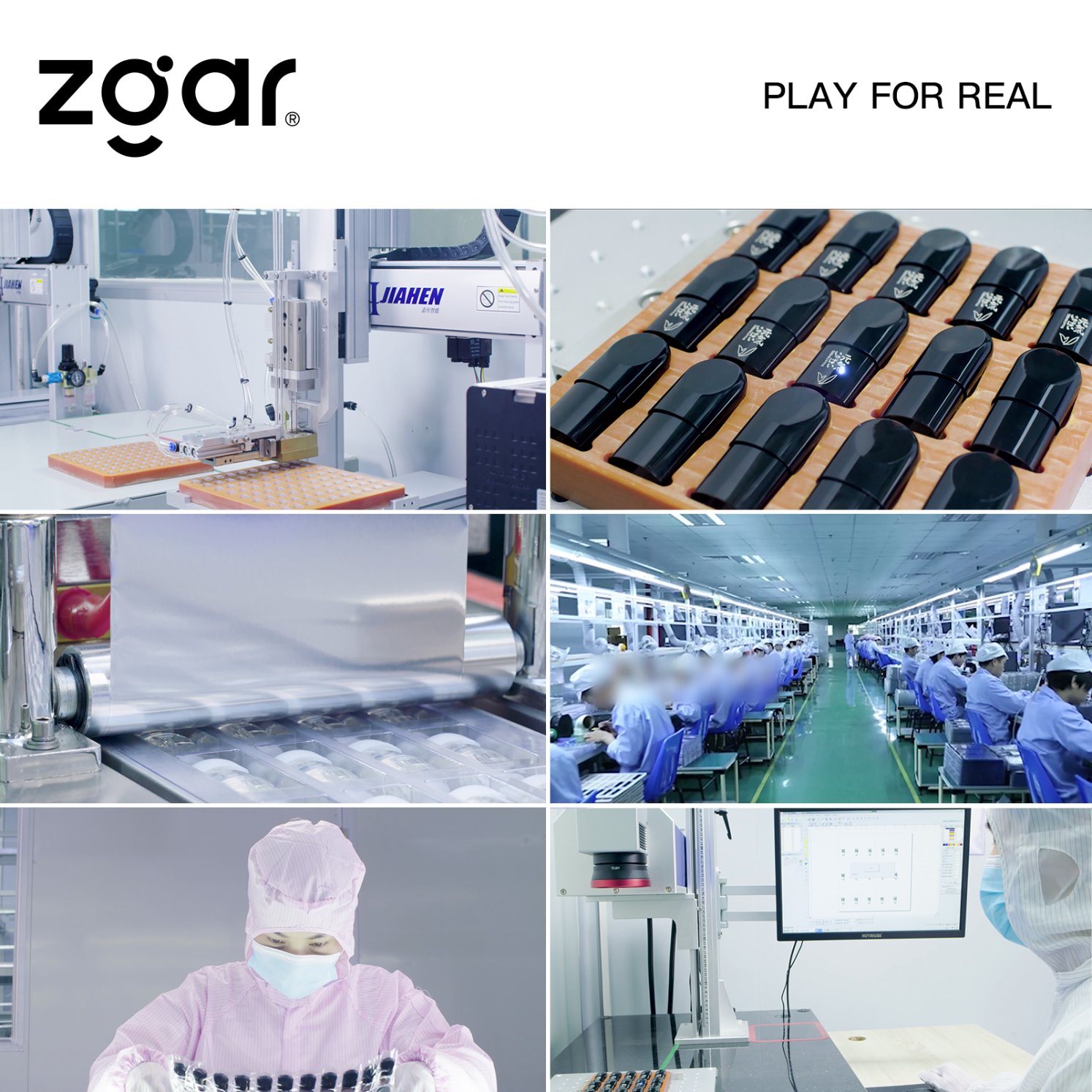
ZGAR electronic cigarette uses high-tech R&D, food grade disposable pod device and high-quality raw material. All package designs are Original IP. Our designer team is from Hong Kong. We have very high requirements for product quality, flavors taste and packaging design. The E-liquid is imported, materials are food grade, and assembly plant is medical-grade dust-free workshops.
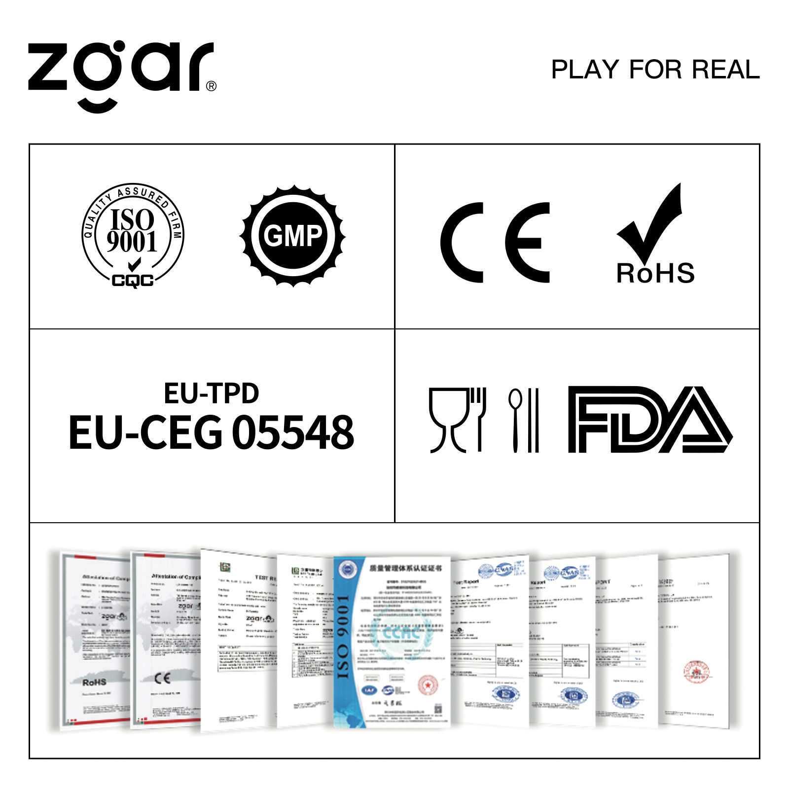
From production to packaging, the whole system of tracking, efficient and orderly process, achieving daily efficient output. WEIKA pays attention to the details of each process control. The first class dust-free production workshop has passed the GMP food and drug production standard certification, ensuring quality and safety. We choose the products with a traceability system, which can not only effectively track and trace all kinds of data, but also ensure good product quality.
We offer best price, high quality Pods, Pods Touch Screen, Empty Pod System, Pod Vape, Disposable Pod device, E-cigar, Vape Pods to all over the world.
Much Better Vaping Experience!


Pods, Vape Pods, Empty Pod System Vape,Disposable Pod Vape Systems
ZGAR INTERNATIONAL TRADING CO., LTD. , https://www.sze-cigarette.com