How does a MEMS device behave in a real world that contains stress factors such as motion, vibration, and temperature fluctuations? One important means of ensuring that the MEMS device's performance in the real environment meets expectations is to perform finite element analysis (FEA). FEA defines a grid on the three-dimensional model of the MEMS device, which subdivides the complex calculations that calculate the influence of physical forces into finite elements. The basic physical mechanism of each finite element is calculated, a complex equation is established, and then the physical effects on the entire design are approximated. This technical paper examines the preparation of FEA by studying tunable optical filters (Figure 1).
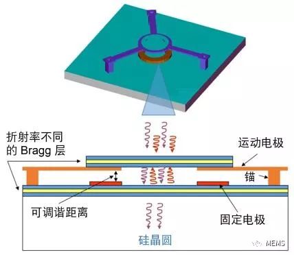
Figure 1: Tunable optical filter
Tunable optical filters are a key component of wavelength division multiplexing (WDM) solutions for building optical fiber communication systems. A Fabry-Perot resonator is constructed using two parallel Bragg mirror layers with different refractive indices. A moving electrode is suspended on three beams. When a voltage is applied, the moving electrode moves to the fixed electrode under the electrostatic force. The distance between the two Bragg layers determines the resonant wavelength frequency. Light waves enter the resonant cavity, but only the resonant wavelength can pass through the resonant cavity.
Can this filter be manufactured? Will it work as expected? To answer these questions, designers may ask:
• Can the tuneable frequency range meet the requirements? • Will the beam bend correctly to filter the beam as expected? • Does the movement of the beam distort the Bragg surface? • Will the beam speed be fast enough to meet the requirements? • Can a beam withstand motion stress without failure? • How does a non-ideal mirror affect the operation of the device?
To answer these questions, FEA tools should be used to simulate the device under actual conditions. The FEA preparations that the designer must complete include specifying the manufacturing process, creating a two-dimensional mask layout, and generating an optimized three-dimensional model of the device in Tanner L-Edit.
Designated manufacturing process
Designers can work with foundries to specify manufacturing processes directly in L-Edit. The first step is to explain the materials used to make the tunable filter: metal, polysilicon, oxide, and nitride. The designer adjusts the material properties as needed, and this information is then passed to the FEA tool. Next, the designer specifies the three-dimensional filter steps associated with the material. Each of the specified steps mimics the machine steps used in manufacturing, such as deposition, etching, polishing, and the like. For example, an etching step is defined after one deposition step, which specifies the material to be etched and the material removed by etching. The designer maps the appropriate process steps to the two-dimensional mask layout. (Real device profiles can be generated) For tunable filters (Figure 2), the basic process steps include:
• Deposits the oxide, polysilicon, and nitride of the mirror. • Etch a layer of polysilicon after deposition. • Deposit oxides and etch the fixed electrodes. • Deposited metal. • Deposits nitrides, oxides, and polysilicon on the top mirror. • Deposit and etch beams, anchors and moving electrodes.

Figure 2: Manufacturing Process Steps for Tunable Filters
Create a two-dimensional mask layout
A filter was created in L-Edit to specify the material layers that form the anchor beam and the upper and lower electrodes on the silicon wafer basis (Figure 3).
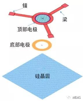
Figure 3: Tunable filter layout
The filter cavity is filled with air. To study the electrostatic behavior of the filter, the designer can add a layer to the two-dimensional layout in L-Edit to handle the amount of air between the two electrodes (Figure 4).
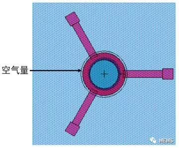
Figure 4: Adding an air layer to the filter layout
Generate 3D models
Designers can start by creating a three-dimensional model of the filter in the FEA tool. However, a two-dimensional mask is required to fabricate the device. Therefore, it is best to begin by creating a two-dimensional mask layout in L-Edit. Then, instruct L-Edit to automatically generate a three-dimensional model through these masks to provide a simulation of the manufacturing steps. With this mask-oriented design flow, designers can focus on designing practical devices because the masks that are ultimately used for manufacturing purposes are created directly, rather than reversed from the 3D model.
Figure 5 shows a three-dimensional model of the tunable filter automatically generated from the two-dimensional mask layout in L-Edit.
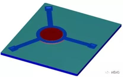
Figure 5: Generated tunable filter 3D model
Designers can examine the manufacturing process steps in a 3D model and take snapshots for documenting. To explore the relationship between the elements in the model, you can specify the model's stack structure (Figure 6).
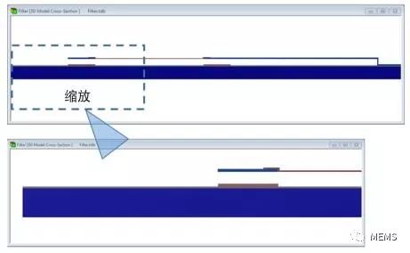
Figure 6: Explore the section of the 3D model
Optimize performance
If MEMS devices are complex, FEA tools may take a long time to complete the simulation and may not even converge. Designers can use a variety of techniques to optimize the simulation performance of 3D models, including:
• Close some of the materials and process steps used in the 3D model and export them to the FEA tool. • Use the feature removal tool in L-Edit to clear holes, merge corner faces, and clear small rounded corners to simplify the model. • A partition of the simulation model for targeted analysis.
Using the L-Edit Substrate function to create a 1/3 partition of the 3D model can simplify the tunable filter. The new model contains only one beam, one-third of the upper and lower electrodes, and one-third of the air volume in the cavity (Figure 7). This partition reduces the size and complexity of FEA analysis. The designer can then perform a targeted analysis of the electrostatic properties of the beam and the electrode.
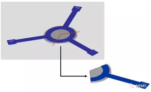
Figure 7: Partitioning a 3D model to improve simulation performance
Follow up steps
After generating an optimized 3D model, the designer can export the description into one of several formats and import the model into the FEA tool. The necessary electrostatic information, boundary conditions, material properties, and beam degrees of freedom are provided by the 3D model.
In the FEA tool, the designer verifies that the filter can work properly within a specified tuning range given a proper beam. In addition, designers can experiment to investigate the effects of mirror defects or mirror curvature on the tuner.
After performing FEA, if any problems are found, modify the 2D model and regenerate the 3D model for FEA. After confirming the physical effects of the design, designers can use the MEMS Modeler tool from SoftMEMS (used with the T-Spice simulator) to generate the behavioral model of the device.
Conclusion
In order to make MEMS devices, important questions must be answered to ensure that the device will work properly under actual conditions. Tanner's mask-oriented design flow associates manufacturing process steps and materials with two-dimensional mask layouts to automatically generate optimized three-dimensional models for finite element analysis. This design process helps to ensure that the manufactured MEMS device meets expectations.
Applause for Obelisk 65, the palm-fit tech-chic gathers GEEKVAPE's most cutting-edge technology.
2-day-use battery life. Stable output with built-in battery.
Easy-to-use pod with leakproof design.
And this tech-chic-looking device fits right in your palm.
Express yourself with the chicest and the latest!
For up to 48 hours, Obelisk 65 can run on a single charge. It still
delivers the same power performance whether the battery is
fully charged or not.
geekvape obelisk series box mod,geekvape obelisk series pod kit,geekvape obelisk series vape kit,geekvape obelisk series mods,geekvape obelisk series disposable
Ningbo Autrends International Trade Co.,Ltd. , https://www.supermosvape.com