This article will discuss how to improve the efficiency of system-level design.
Today, many analog, RF, and mixed-signal designs require the integration of multiple ICs in different substrate technologies to achieve the required performance goals.
In view of the complexity of today's chips, packages, and circuit boards, not only silicon but also other non-silicon materials need to be used in the design to achieve optimal system performance. The integration of heterogeneous devices allows designers to achieve design results that cannot be easily replicated with monolithic IC (SoC) design methods. However, heterogeneous integration also brings new challenges for designers.
Today, designing at the "system level" (IC-package-PCB) involves a lot of empirical guesses about the impact of downstream packaging/PCB on chip performance and reliability. Traditionally, analog/RF IC designers only need to simulate the IC without considering the impact of packaging and PCB. Generally speaking, however, a package contains one or more ICs and interconnect components, and sometimes may also contain discrete components required for IC operation; similarly, a PCB also contains multiple packages, interconnects, and discrete components. Therefore, unifying the entire system for simulation is very important for capturing high frequency performance. Since IC designers and package designers use different schematic input tools, IC designers have to recapture the package system schematic and place it on the IC schematic test platform before they can simulate the joint system.

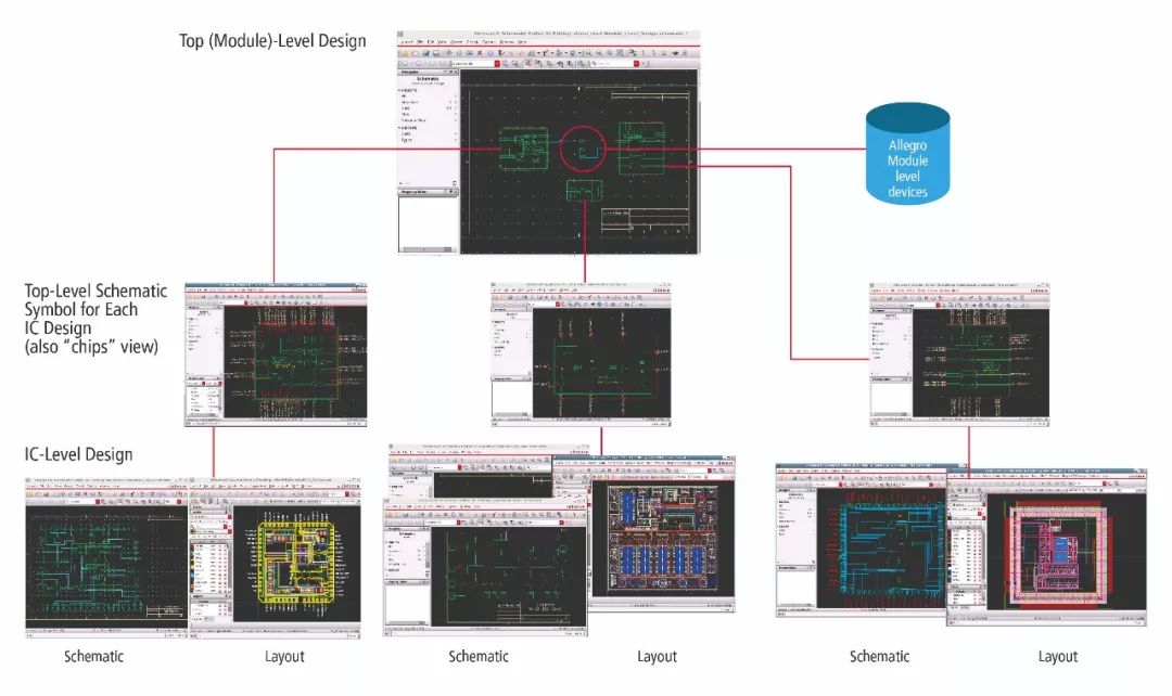
Figure 1: Virtuoso system design platform
This process provides the ability to drive IC and package layout through a single schematic editor. By using the same schematic editor (Virtuoso Schematic Editor), IC designers can better perform system-level design in a common environment, including pre-wiring system simulation (IC and package together), and then drive the wiring in their respective fields. The process also automates the development process of most package-level libraries by generating chip pins used in Cadence SiP Layout.
Co-design between chip and package
High-end users can design collaboratively between chip and package to achieve better package-level wiring and/or wire bonding. This process allows designers to put the packaged schematic diagram into the Virtuoso Schematic Editor for design before package placement and routing. Furthermore, you can export the chip pins and symbols from the Virtuoso Layout kit and use them to build package schematics. The two-way flow of data can dynamically transfer the edits made in the schematic to the SiP Layout and vice versa. Designers can also generate bills of materials, visualize design differences in an intuitive way, and use this process to view layout reports.

Figure 2: RS Pro Evikey
Once the package or PCB is designed by the process, the analysis-based process will be brought into a complete simulation environment, which can be easily completed without professional knowledge of PCB or packaging and electromagnetic simulation. This method will significantly increase productivity. This analysis process allows IC designers to import PCB and package layouts and their corresponding parasitic models (expressed in S-parameters or SPICE) into the IC design environment, then read the PCB or package connections and create a schematic diagram containing the parasitic model . The schematic can be simulated at any time in the environment of the PCB or packaging system.
This design platform facilitates the integration and simulation of ICs with the inclusion of package/PCB interconnection and external components. Since IC, package, and PCB are usually designed by different teams in different geographic locations using different design tools, and are independent at different stages of the design cycle, this design platform is particularly important. The platform incorporates the package and PCB-level layout parasitics into the general schematic diagram to realize the cross-region simulation of the entire system. This helps identify critical performance deviations before tape out.
Then, the required modification information can be passed directly to the packaging/PCB team. There is an important function here, that is, the parasitic model can be intelligently integrated into the simulation schematic. If the model also contains discrete devices, they will be automatically filtered out when creating the simulation circuit diagram, so that they will not be recalculated in the simulation. Automatic filtering requires re-adjusting the interface to ensure proper integration and remove all SMD to avoid redundancy.
Having such a powerful integrated platform can bring designers the following three advantages:
By using the general schematic editor, designers can now design schematics for packaged layouts. Virtuoso Schematic Editor is a unified schematic editor that can drive IC and package design.
Designers can create schematic diagrams of packages or PCBs with parasitic effects, and use Virtuoso Analog Design Environment for simulation. The multi-technology simulation included is an important mechanism to achieve complete system simulation.
Designers can simultaneously design IC and package layout through the brief process of co-designing chips, minimizing the number of design iterations and reducing later layout planning and design feasibility issues.
In short, the Virtuoso System Design Platform is a comprehensive, system-based solution that enables simulation of ICs and packages driven by a single schematic, and LVS inspection.

The design platform won the Electronic Products of the Year Award from the Electronic Products website in 2017.
China Area Array Sensor
Area Array Sensor,Passive Infrared Detector,Infrared Heat Detector,Infrared Area Sensor
Ningbo NaXin Perception Intelligent Technology CO., Ltd. , https://www.nicswir.com