Radio Frequency Identification (RFID) is a rapidly developing automatic identification technology that has emerged in recent years. It uses radio frequency methods for non-contact two-way communications to achieve the purpose of identification and exchange data. RFID is the basis of high-tech and information standardization for rapid, real-time, accurate information collection and processing, and has broad application prospects in various industries such as production, retail, logistics, and transportation. RFID technology has been recognized by the world as one of the ten most important technologies of this century.
The RFID tag contains an antenna and a chip, both of which have complex impedances. For passive tags, because the power consumption required for tag operation all comes from the RF energy emitted by the reader, whether the antenna and the chip can achieve good matching and power transmission directly affects the realization of system functions. It largely determines the key performance of the tag.
The existing impedance matching methods are mostly complex, and the accuracy of tag identification is low when used in RFID chips, and the effect is not ideal. A method of designing a low-cost impedance matching network for passive RFID tag chips is proposed in the article. The matching network is integrated in the tag chip and has a simple structure. It is implemented between the tag antenna and the chip and between the tag and the reader. The maximum power transfer improves chip performance and improves reader identification of tag reflected signals.
1 RFID tag impedance matching analysis1.1.1 RFID principle and label composition
Common RFID systems consist of readers and tags. The reader sends a continuous wave of radio frequency (CW) to the tag, activates the tag chip, and modulates the commands and data into the radio frequency electromagnetic wave. The tag in the electromagnetic field of the reader writer increases the small input voltage to the voltage value required for the normal operation of the tag chip through the voltage doubler rectifying circuit, and converts the AC to DC; since the chip input voltage varies widely Causes the output voltage to be unstable and needs to be added to the regulator circuit; the tag demodulation module demodulates commands and data from the received RF continuous wave and sends it to the digital baseband module; the digital baseband module completes the received command according to the protocol. Data storage, transmission or other operations [4]; when returning data, the tag changes the antenna's reflection coefficient by changing its own impedance and sends the modulated reflection signal back to the reader. The clock generation circuit provides the clock frequency required for the chip operation and is calibrated by the clock calibration information sent by the reader/writer to achieve clock synchronization. The power-on reset circuit resets the baseband processor on the one hand, and provides an enable for the modulation and reflection circuit on the other hand. signal.
Figure 1 shows the block diagram of the RFID tag system. The chip contains three parts: RF analog front end, digital baseband, and non-volatile memory (NVM). The analog front-end basic functional modules include: impedance matching, voltage doubler rectification, modulation, demodulation, voltage regulation, power-on reset, clock generation, and so on.
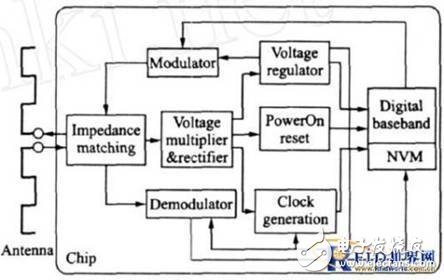
Figure 1 Block diagram of radio frequency identification tag system
1.1.2 Impedance Matching Analysis
Figure 2 shows the Thevenin equivalent circuit of the tag, which has been used by many researchers to solve various antenna problems. The open circuit AC voltage induced by the RF signal on the antenna is Va, the chip input voltage is Vc, the antenna input impedance Za=Ra+jXa, and the chip input impedance Zc=Rc+jXc. The real part of the chip input impedance is mainly determined by the voltage doubler rectifier circuit and the load, and the imaginary part is mainly determined by the voltage doubler rectifier circuit, the modulation and demodulation circuit and the ESD. Both Za and Zc change with the operating frequency, and in practical applications, the values ​​of Zc vary with different input powers. In this paper, the impedance matching network is designed under the condition that the input power is equal to the minimum power required for the normal operation of the chip. For maximum power transfer, the chip's input impedance must be conjugate to the antenna.
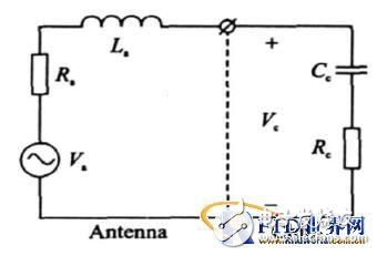
Figure 2 Equivalent Circuit of RFID Tag
L-type matching is an impedance matching method used to achieve high-efficiency radio-to-DC conversion. The purpose of matching is achieved through the series inductance and the capacitance resonance in the chip. For RFID tag chips, integrating the inductor in a small area is unrealistic. Therefore, the input impedance of the chip is modified by the following method to achieve the purpose of L-type matching using the inductance La.
When two devices with complex impedances are directly connected, the complex power wave reflection coefficient at the interface is defined as s, which can be obtained when applied to RFID tags:

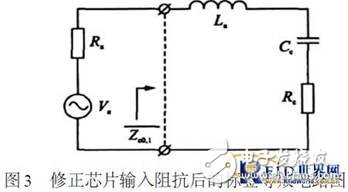
When the chip is in conjugate matching (state 0) and mismatch (state 1) with the antenna impedance, the corresponding input impedances are Zc0 and Zc1 respectively. Through the impedance correction, the imaginary part of the antenna impedance is added to the chip, and the corrected antenna impedance is only The real part Ra is retained, as shown in Figure 3. The input voltage of the chip can be calculated by formula (3):

Because the energy required for the passive RFID chip to work completely comes from the space electromagnetic field, the input voltage Vc has a sufficiently high value that the voltage doubler rectifier circuit can be turned on and provide the normal working voltage, and is also an important parameter that determines the work performance of the tag.
The RCS (Radar Scattering Cross Section) of the RFID tag is a function of the input impedance of the chip. The RCS value can be obtained from the classical radar equation:

Where K is the wavelength and G is the tag antenna gain. Corresponding different RCS values ​​for the two chip input impedance states allow the reader to resolve the tag transmitted data from the modulated reflected signal amplitude. The vector differential RCS further allows the reader to detect the relative phase characteristics of the modulated reflected signal. The module of this vector is labeled with ΔV:

2.1.1 Principle Analysis
When the tag works in the 923MHz band, the chip is in the minimum input power, unmodulated state, using the Agilent E5071C network analyzer to measure the input impedance of the chip that is not added to the impedance matching network as 22-j106 ohms. According to the input impedance characteristics of the chip, a tag antenna with a larger Q value is selected. The input impedance of the antenna is 15+j88 ohms. The design of the impedance matching network is shown in Fig. 4, where La=1512nH.
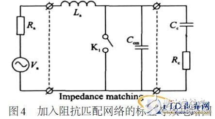
When the switch K1 is off, the chip is in state 0. In the matching path from the input impedance of the tag chip to the conjugate impedance of the antenna shown in FIG. 5, the impedance at point 1 is 22-j 106 ohms; after the parallel capacitance Ccm and the resistance circle 158 intersect at point 2, the impedance is 15- J888; series inductor La reaches point 3, its impedance is 158, and the modified antenna impedance Ra conjugate matches. It is calculated that Ccm = 340fF.
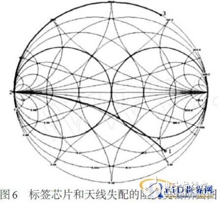
There is no reflection of complex power waves at the interface between the antenna and the chip. The conjugate matching between the chip and the antenna allows the antenna to transmit half of the RF energy received from the air to the chip, thus maximizing the power transmission. When the switch K1 is closed, the chip is in state 1. Figure 6 shows the path of the input impedance of the tag chip.

2.1.2 Performance Comparison
In the absence of impedance matching, the value of the chip Qc is 4182. After the impedance matching network is added, the Qc increases to 5187 under the state of the conjugate and matching of the impedance of the chip and the antenna, and the AC obtained by the formula (3) can be obtained. The voltage Vc increases by a factor of 111, improving the performance of the chip.
By comparison, the module's vector differential RCS has a large modulus of 1015dB, which greatly improves the recognizability of the tag's reflected signal and improves the reader's accuracy in tag identification.
2.1.3 circuit implementation
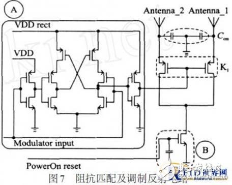
The impedance matching network is composed of a capacitor Ccm and a switch K1, as shown in FIG. 7. In order to ensure the symmetry of the circuit between the two antenna pins, Ccm uses two capacitors in parallel, each with a size of 170fF; K1 consists of two PMOS switches and the PMOS consists of the baseband signal through a level shifter (Figure 7A). Part) after the drive, so the gate of the PMOS can get a higher gate voltage to ensure the reliable shutdown of the off state; part B is the power-on protection circuit to ensure that the power-on reset signal given by the digital baseband is in a stable state. Entering the modulation reflection avoids the chip from reflecting when it cannot obtain working energy due to the uncertainty of the state before the digital baseband circuit is reset. Both the PMOS switch and the NMOS power-up protection tube adopt a mesh gate structure, and increasing the width-length ratio of the MOS tube is advantageous to reduce the resistance and parasitic capacitance of the MOS tube.
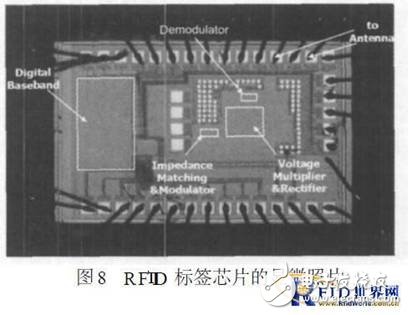
The designed RFID tag chip is based on charted0135Lm2P4M, low threshold CMOS process chip, chip size 1026Lm & TImes; 1796Lm, Figure 8 is a micrograph of the chip. In actual use, only two pins of the chip are connected to the antenna. The rest of the pins shown in the figure are used for testing and are connected to corresponding analog or digital signals.
The output level of the voltage doubler circuit is an important indicator to determine the working performance of the RFID chip. When the chip with this impedance matching circuit is only 300mV at the input AC level, the output DC level can reach 1147V, which fully meets the required level of the chip for normal operation. . The RFID operating frequency band specified in 1800026C is 860-960 MHz, and coincides with the regulations of China [11] in the 920-925 MHz frequency band. Therefore, the designed RFID tag operates in the 923 MHz frequency band.
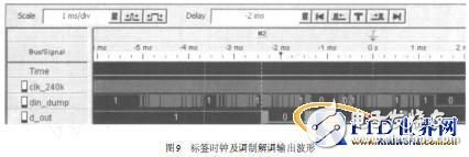
Using Impinj's speedway reader, set the transmit power to 2 WERP and the tag antenna gain to 115 dBi to test in free space. Using the Agilent 1682A logic analyzer to test signal waveforms as shown in Figure 9, the figure "clk-240k" is the system clock, the frequency is 240kHz; "din-dump" is the demodulated output signal; "d-out" is the modulated output signal. Tests have shown that during the process of communicating with readers using the impedance matching network, the bit error rate is lower than 10-4, and the identification of tags is more accurate.
A low-cost impedance matching network for passive RFID tags conforming to the ISO1800026C standard is proposed. The circuit structure is simple, and the power transmission is maximized between the reader/writer, the tag antenna and the chip. The tag chip using this impedance matching method has been verified by taped 0135LmCMOS process. Both the theoretical analysis and the measured results show that this method can effectively improve the performance of the chip, improve the reader's accuracy of tag identification, and the tag meets the system design requirements.
Large Servo Drives,Digital Ac Servo Driver,Variable Frequency Drives,Full Closed Loop Servo Driver
Zhejiang Synmot Electrical Technology Co., Ltd , https://www.synmot-electrical.com