Abstract: This article discusses the application of the EIA / TIA-644 low-voltage differential signaling (LVDS) standard in 3G mobile communication equipment. LVDS has the advantages of low power consumption and low radiation, and can be ideally used for high-speed in W-CDMA, EDGE and CDMA2000 Clock and data transmission.
3G mobile communications, such as W-CDMA, EDGE and CDMA2000, allow our mobile phones to access the rich and colorful Internet world at high speed. To meet this bandwidth requirement, base stations (interfaces of wireless handheld devices and wired networks) must process and send huge amounts of data that grow exponentially.
Inside the base station, these data are transmitted at high speed on the backplane, cable, and circuit board. Low-voltage differential signaling (LVDS) will become the signal standard for transmitting these data. It reduces space, noise, and power consumption. These parameters are more demanding in base station design.
This application note discusses the applications of LVDS serializers, deserializers, multi-port repeaters, crosspoint switches, and level shifters in data and clock distribution. Focus on discussing LVDS circuits, architecture, and specifications related to 3G base station design.
LVDS is a physical layer data interface standard defined by the TIA / EIA-644 and IEEE 1596.3 standards. It is mainly designed to achieve high-speed, low-power, and low-noise point-to-point communication on a 100Ω medium with a balanced impedance controllable. As with other differential signal standards, LVDS eliminates magnetic fields and is much less noisy than single-ended signals. At the same time, external noise is coupled to the two lines as a common-mode signal (that is, the noise level on both lines is the same), so its anti-noise ability is much stronger than that of single-ended signals. In addition, the output of the LVDS driver uses a current drive method (Figure 1). Compared with the voltage drive in other differential signal standards, it reduces ground return and eliminates inrush current. Reducing the voltage swing (only ± 350mV, PECL is ± 800mV, RS-422 is 2V) enables LVDS to achieve the same data rate as PECL (> 800Mbps), and the power consumption is only one tenth of PECL. The high speed, low power consumption and low noise characteristics of LVDS make it an ideal standard for 3G base station signal transmission.
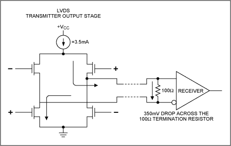
Figure 1. The LVDS driver is driven by current output. Compared with the voltage mode used by other differential signals, it can reduce the influence of ground potential deviation and also eliminate the punch-through current.
In addition to the above advantages, LVDS serializers and deserializers also save a lot of space and money for base station design. In order to meet the broadband requirements of the 3G network, the new base station requires a large number of boards compared to the 2G system-especially the baseband processing board, which is responsible for heavy digital signal processing tasks such as spreading, interleaving and error control. As the data throughput between these boards increases, traditional TTL backplanes are no longer competent, because firstly TTL logic is not suitable for higher operating speeds, and secondly, wide parallel buses require large and expensive backplanes, which leads to the entire system Increase and cost increase. Maxim's MAX9205 serializer and MAX9206 deserializer effectively solve the above problems by converting 11 TTL lines (10 data and 1 clock) into a pair of high-speed LVDS lines (Figure 2). Using this scheme can reduce the interconnect density by 5 times. In 3G systems and other base stations with a large number of boards, these products can save a lot of space and costs.
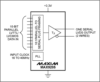
Figure 2. An LVDS serializer with a deserializer (not shown) can effectively save wide data lines and related, expensive, backplanes required for standard TTL signals. In addition, LVDS can meet the speed required by 3G networks.
The MAX9205 serializer converts 10-bit parallel LVTTL / LVCMOS data into an LVDS serial data stream. A high-level start bit and a low-level stop bit are added to 10-bit data to form a serial data frame. So every 10 bits of data send 12 bits of information. The MAX9205 allows a 16-40MHz reference clock to be input, and the corresponding serial data rate from 192Mbps (12-bit x 16MHz) to 480Mbps (12-bit x 40MHz). Since only 10 bits are input data, the actual throughput is 10 times the clock frequency. The MAX9206 deserializer receives the serial output of the MAX9205 and converts it back to 10-bit parallel data. Because the deserializer simultaneously recovers the clock and data from the serial data stream, it eliminates the clock-data and data-data offsets common in parallel buses. The MAX9205 and MAX9206 provide a complete solution for reducing the interconnection density between boards. Because 3G base stations usually use one-way connection, it is very suitable for 3G base stations to use two ICs to complete these functions. Next, only a deserializer is needed on the baseband board, compared to the integrated serial deserializer, which wastes extra space and expense.
In base stations that have adopted serial backplanes, an LVDS multiport repeater can further reduce board space and cost. In most base stations, some boards must broadcast or send data to multiple boards. Many systems use multiple baseband boards to process data sent by an RF transceiver in parallel. The worst solution is to use the same number of serializers on the RF board as the baseband board deserializer (Figure 3a). If a multipoint repeater such as the MAX9150 is used, the number of serializers will drop significantly to one-tenth of the original (Figure 3b). The MAX9150 can be used with a serializer to replace 10 serializers. This structure is effective only when the multipoint repeater has sufficiently low jitter characteristics. Jitter is the degree of deviation from the ideal timing of an event or signal edge. It affects the deserializer's successful recovery of clock and data from the serial bit stream. The jitter margin of a typical LVDS serializer / deserializer pair is as low as a few hundred ps, and this margin will be further reduced by the effects of wiring, cables, and connectors. Therefore, other devices on the signal path between the serializer and deserializer must have particularly low jitter. The maximum peak-to-peak jitter of the MAX9150 is only 120ps, which is lower than the jitter specifications of any multipoint repeater on the market.
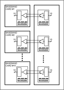
Figure 3a. When multiple baseband cards receive data from a wireless transceiver card, the number of serializers included in the wireless communication card is the same as the number of deserializers at the baseband card of the terminal.
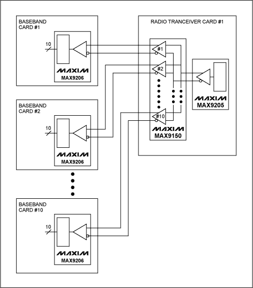
Figure 3b. Using a multi-port repeater (MAX9150), the number of serializers in a wireless transceiver card can be reduced by 10: 1.
In other parts of the high-speed serial signal channel, the base station structure usually requires some simple switching, multiplexing, and relay functions. As with multipoint repeaters, the impact of these increased functions on the jitter margin must be as small as possible. The MAX9152 2x2 LVDS crossbar provides several functions in one device. It includes two LVDS / LVPECL inputs, two LVDS outputs, and two logic inputs to determine the connection between the input and output. It can be programmed to connect either input to either output or both outputs. So it can be configured as a 2x2 crossbar switch, 2: 1 multiplexer, 1: 2 demultiplexer, 1: 2 fan-out buffer or two repeaters. This versatile feature makes the MAX9152 an ideal choice for fault redundancy protection switching, self-diagnostic loopback switching, fan-out buffering during data distribution, and signal regeneration during ultra-long-distance communications.
In low-speed signal channels, such as clock distribution networks and control buses, using LVDS to replace early signal standards such as TTL and RS-422 can effectively improve the performance indicators of the corresponding systems. The base station RF transceiver board is particularly sensitive to radiated noise. LVDS is an ideal signal standard for distributing the reference clock used by the PLL frequency synthesizer. Although these circuits do not require the high-speed performance of LVDS (the typical value of the base station reference clock is tens of MHz), they benefit from the low power consumption and low radiation noise of LVDS. The low-speed control bus used for arbitration, handshake and other peripheral communication between boards can also benefit from the reduction of noise and power consumption. The level shifter is only used for signal conversion between LVTTL / LVCMOS and LVDS, and provides us with a simple method to construct an LVDS clock distribution network and control bus from the existing LVTTL / LVCMOS design. Maxim's single, dual, and quad drivers and receivers are ideal choices, with features such as small size (SC70 and SOT23 packages) and low pulse offset (pulse skew is the main measure of jitter performance in these devices). .
Leveraging the advantages of LVDS in the fields of clock distribution, control bus, backplane and other high-speed signal transmission, 3G base stations will bring bandwidth wireless services without increasing costs, size and power consumption in proportion. The products discussed in this article provide these advantages not only in the form of LVDS signal standards but also in the structure and layout they support. A comprehensive understanding of LVDS technology, products, and applications is the basis for engineers to develop next-generation cellular base stations.
3G mobile communications, such as W-CDMA, EDGE and CDMA2000, allow our mobile phones to access the rich and colorful Internet world at high speed. To meet this bandwidth requirement, base stations (interfaces of wireless handheld devices and wired networks) must process and send huge amounts of data that grow exponentially.
Inside the base station, these data are transmitted at high speed on the backplane, cable, and circuit board. Low-voltage differential signaling (LVDS) will become the signal standard for transmitting these data. It reduces space, noise, and power consumption. These parameters are more demanding in base station design.
This application note discusses the applications of LVDS serializers, deserializers, multi-port repeaters, crosspoint switches, and level shifters in data and clock distribution. Focus on discussing LVDS circuits, architecture, and specifications related to 3G base station design.
LVDS is a physical layer data interface standard defined by the TIA / EIA-644 and IEEE 1596.3 standards. It is mainly designed to achieve high-speed, low-power, and low-noise point-to-point communication on a 100Ω medium with a balanced impedance controllable. As with other differential signal standards, LVDS eliminates magnetic fields and is much less noisy than single-ended signals. At the same time, external noise is coupled to the two lines as a common-mode signal (that is, the noise level on both lines is the same), so its anti-noise ability is much stronger than that of single-ended signals. In addition, the output of the LVDS driver uses a current drive method (Figure 1). Compared with the voltage drive in other differential signal standards, it reduces ground return and eliminates inrush current. Reducing the voltage swing (only ± 350mV, PECL is ± 800mV, RS-422 is 2V) enables LVDS to achieve the same data rate as PECL (> 800Mbps), and the power consumption is only one tenth of PECL. The high speed, low power consumption and low noise characteristics of LVDS make it an ideal standard for 3G base station signal transmission.

Figure 1. The LVDS driver is driven by current output. Compared with the voltage mode used by other differential signals, it can reduce the influence of ground potential deviation and also eliminate the punch-through current.
In addition to the above advantages, LVDS serializers and deserializers also save a lot of space and money for base station design. In order to meet the broadband requirements of the 3G network, the new base station requires a large number of boards compared to the 2G system-especially the baseband processing board, which is responsible for heavy digital signal processing tasks such as spreading, interleaving and error control. As the data throughput between these boards increases, traditional TTL backplanes are no longer competent, because firstly TTL logic is not suitable for higher operating speeds, and secondly, wide parallel buses require large and expensive backplanes, which leads to the entire system Increase and cost increase. Maxim's MAX9205 serializer and MAX9206 deserializer effectively solve the above problems by converting 11 TTL lines (10 data and 1 clock) into a pair of high-speed LVDS lines (Figure 2). Using this scheme can reduce the interconnect density by 5 times. In 3G systems and other base stations with a large number of boards, these products can save a lot of space and costs.

Figure 2. An LVDS serializer with a deserializer (not shown) can effectively save wide data lines and related, expensive, backplanes required for standard TTL signals. In addition, LVDS can meet the speed required by 3G networks.
The MAX9205 serializer converts 10-bit parallel LVTTL / LVCMOS data into an LVDS serial data stream. A high-level start bit and a low-level stop bit are added to 10-bit data to form a serial data frame. So every 10 bits of data send 12 bits of information. The MAX9205 allows a 16-40MHz reference clock to be input, and the corresponding serial data rate from 192Mbps (12-bit x 16MHz) to 480Mbps (12-bit x 40MHz). Since only 10 bits are input data, the actual throughput is 10 times the clock frequency. The MAX9206 deserializer receives the serial output of the MAX9205 and converts it back to 10-bit parallel data. Because the deserializer simultaneously recovers the clock and data from the serial data stream, it eliminates the clock-data and data-data offsets common in parallel buses. The MAX9205 and MAX9206 provide a complete solution for reducing the interconnection density between boards. Because 3G base stations usually use one-way connection, it is very suitable for 3G base stations to use two ICs to complete these functions. Next, only a deserializer is needed on the baseband board, compared to the integrated serial deserializer, which wastes extra space and expense.
In base stations that have adopted serial backplanes, an LVDS multiport repeater can further reduce board space and cost. In most base stations, some boards must broadcast or send data to multiple boards. Many systems use multiple baseband boards to process data sent by an RF transceiver in parallel. The worst solution is to use the same number of serializers on the RF board as the baseband board deserializer (Figure 3a). If a multipoint repeater such as the MAX9150 is used, the number of serializers will drop significantly to one-tenth of the original (Figure 3b). The MAX9150 can be used with a serializer to replace 10 serializers. This structure is effective only when the multipoint repeater has sufficiently low jitter characteristics. Jitter is the degree of deviation from the ideal timing of an event or signal edge. It affects the deserializer's successful recovery of clock and data from the serial bit stream. The jitter margin of a typical LVDS serializer / deserializer pair is as low as a few hundred ps, and this margin will be further reduced by the effects of wiring, cables, and connectors. Therefore, other devices on the signal path between the serializer and deserializer must have particularly low jitter. The maximum peak-to-peak jitter of the MAX9150 is only 120ps, which is lower than the jitter specifications of any multipoint repeater on the market.

Figure 3a. When multiple baseband cards receive data from a wireless transceiver card, the number of serializers included in the wireless communication card is the same as the number of deserializers at the baseband card of the terminal.

Figure 3b. Using a multi-port repeater (MAX9150), the number of serializers in a wireless transceiver card can be reduced by 10: 1.
In other parts of the high-speed serial signal channel, the base station structure usually requires some simple switching, multiplexing, and relay functions. As with multipoint repeaters, the impact of these increased functions on the jitter margin must be as small as possible. The MAX9152 2x2 LVDS crossbar provides several functions in one device. It includes two LVDS / LVPECL inputs, two LVDS outputs, and two logic inputs to determine the connection between the input and output. It can be programmed to connect either input to either output or both outputs. So it can be configured as a 2x2 crossbar switch, 2: 1 multiplexer, 1: 2 demultiplexer, 1: 2 fan-out buffer or two repeaters. This versatile feature makes the MAX9152 an ideal choice for fault redundancy protection switching, self-diagnostic loopback switching, fan-out buffering during data distribution, and signal regeneration during ultra-long-distance communications.
In low-speed signal channels, such as clock distribution networks and control buses, using LVDS to replace early signal standards such as TTL and RS-422 can effectively improve the performance indicators of the corresponding systems. The base station RF transceiver board is particularly sensitive to radiated noise. LVDS is an ideal signal standard for distributing the reference clock used by the PLL frequency synthesizer. Although these circuits do not require the high-speed performance of LVDS (the typical value of the base station reference clock is tens of MHz), they benefit from the low power consumption and low radiation noise of LVDS. The low-speed control bus used for arbitration, handshake and other peripheral communication between boards can also benefit from the reduction of noise and power consumption. The level shifter is only used for signal conversion between LVTTL / LVCMOS and LVDS, and provides us with a simple method to construct an LVDS clock distribution network and control bus from the existing LVTTL / LVCMOS design. Maxim's single, dual, and quad drivers and receivers are ideal choices, with features such as small size (SC70 and SOT23 packages) and low pulse offset (pulse skew is the main measure of jitter performance in these devices). .
Leveraging the advantages of LVDS in the fields of clock distribution, control bus, backplane and other high-speed signal transmission, 3G base stations will bring bandwidth wireless services without increasing costs, size and power consumption in proportion. The products discussed in this article provide these advantages not only in the form of LVDS signal standards but also in the structure and layout they support. A comprehensive understanding of LVDS technology, products, and applications is the basis for engineers to develop next-generation cellular base stations.
Power Bank With Cable,Samsung Mini Power Bank,Powerbank with Built in Cable,Portable Charger with Built in Cable
Pogo Technology International Ltd , https://www.pogomedical.com