1. Abstract
Recently, LLC topology has been favored by many power supply design engineers for its high efficiency and high power density. However, this soft-switching topology requires more MOSFETs than any hard-switching topology. Especially in the power starter, dynamic load, overload, short circuit and other circumstances. With its fast recovery body diodes, low Qg and Coss, CoolMOS can fully meet these requirements and greatly increase the reliability of the power system.
For a long time, improving the power system power density, efficiency and system reliability has always been a major issue for R&D personnel. Raising the switching frequency of the power supply is one of the methods, but the increase of the frequency will affect the switching loss of the power device, so that the lifting frequency is not very obvious for the hard switching topology, and the hard switching topology has reached its design bottleneck. . At this time, soft-switching topologies, such as the LLC topology, are sought after by design engineers because of their unique features. But... This topology puts new demands on power devices.
2. Features of LLC Circuit
The following features of the LLC topology make it widely used in various switching power supplies:
1. The LLC converter can achieve zero voltage switching over a wide load range.
2. The output can be regulated when the input voltage and load vary over a wide range, while the switching frequency is relatively small.
3. Using frequency control, the duty cycle of both the upper and lower tubes is 50%.
4. Reduce the voltage stress of the secondary synchronous rectifier MOSFET, can use lower voltage MOSFET to reduce the cost.
5. No output inductor is required, which can further reduce system cost.
6. Using a lower voltage synchronous rectifier MOSFET can further increase efficiency.
3. The basic structure and working principle of the LLC circuit
Figure 1 and Figure 2 show the typical line and working waveforms of the LLC resonant converter, respectively. The LLC converter shown in Fig. 1 includes two power MOSFETs (Q1 and Q2) with a duty cycle of 0.5, a resonant capacitor Cr, a center-tapped transformer Tr having the same number of secondary turns, an equivalent inductor Lr, and an exciting inductor Lm. Full-wave rectifier diodes D1 and D2 and output capacitor Co.
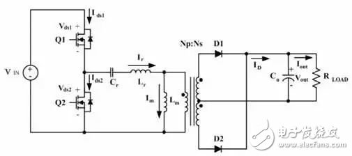
Figure 1 Typical line of an LLC resonant converter

Figure 2 The working waveform of the LLC resonant converter
LLC has two resonance frequencies, Cr, Lr determine the resonance frequency fr1; and Lm, Lr, Cr determine the resonance frequency fr2.
When the load of the system changes, the operating frequency of the system changes. When the load increases, the switching frequency of the MOSFET decreases, and when the load decreases, the switching frequency increases.
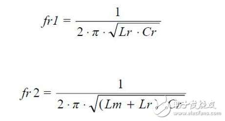
3.1 Operating Sequence of LLC Resonant Converter
The steady-state operation of the LLC converter is as follows.
1) [t1,t2]
Q1 turns off and Q2 turns on. The inductors Lr and Cr resonate. The secondary D1 turns off and D2 turns on. The diode D1 is about twice the output voltage. At this time, the energy is converted from Cr, Lr to the secondary. Until Q2 shuts down.
2) [t2,t3]
Q1 and Q2 are turned off at the same time. At this time, they are in dead time. At this time, the inductor Lr, Lm current charges the output capacitor of Q2 and discharges the output capacitor of Q1 until the voltage of the Q2 output capacitor is equal to Vin.
Secondary D1 and D2 turn off Vd1 = Vd2 = 0, this phase ends when Q1 turns on.
3) [t3,t4]
Q1 turns on and Q2 turns off. D1 is on, D2 is off, Vd2=2Vout
Cr and Lr resonate at fr1, at which point the current of Ls returns to Vin through Q1 until the current of Lr is zero.
4)[t4,t5]
Q1 is on, Q2 is off, D1 is on, D2 is off, Vd2=2Vout
Cr and Lr resonate at fr1, and the current of Lr reversely flows back through Q1 to power ground. Energy is switched from input to secondary until Q1 turns off the phase
5)[t5,t6)
Q1 and Q2 are turned off at the same time. D1 and D2 are turned off. The primary current I (Lr+Lm) charges Q1's Coss and discharges Coss2 until Q2's Coss voltage is zero. At this point, the Q2 diode starts to conduct. The phase ends when Q2 turns on.
6)[t6,t7]
Q1 turns off, Q2 turns on, D1 turns off, D2 turns on, Cr and Ls resonate at frequency fr1, and Lr current returns to ground via Q2. The phase ends when the Lr current is zero.
3.2 Analysis of Abnormal State of LLC Resonant Converter
The above description is that LLC works in resonant mode. Next we analyze the operation of the LLC converter under starter, short circuit, and dynamic load.
3.21 starter status analysis
Through the LLC simulation, we get the waveform shown in Fig. 3. In the first switching cycle of the start-up, the upper and lower tubes will have a short peak current Ids1 and Ids2. Since the MOSFET Q1 turns on, it will give the output capacitance Coss of the lower tube Q2. Charging, charging ends when Vds is high. The peak currents Ids1 and Ids2 are also generated due to Vin charging the Q2 junction capacitance Coss through the MOSFET Q1.
Figure 3 LLC simulation waveform
We will focus on the second switching cycle as shown in Figure 4. We find that similar peak currents will appear at the same time as the first switching cycle, and the peak value will be higher. At the same time, the MOSFET Q2 Vds will also show a very high dv. /dt peak voltage. So is this peak current still caused by Coss? Let's do further research.
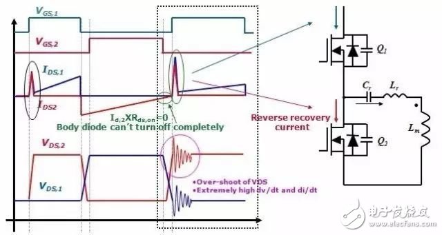
Figure 4 The second switching cycle waveform
Engineers with a certain understanding of the MOSFET structure know that MOSFETs are different from IGBTs. In fact, inside a MOSFET, there is a body diode parasitic. Just like ordinary diodes, neutral carriers need to be reversed during the turn-off process, and only the diode ends. Adding a reverse voltage enables this reverse recovery to be completed quickly, and the energy required for reverse recovery is related to the charge quantity Qrr of the diode. The reverse recovery of the body diode also requires adding a reverse to both ends of the body diode. Voltage. The voltage across the diode at start-up is Vd = Id2 x Ron. While Id2 is almost zero at start-up, the diode requires a long time for reverse recovery when Vd is low. If the dead time is not set enough, the high dv/dt shown in Figure 5 will directly trigger the BJT in the MOSFET to break through the MOSFET.
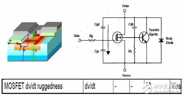
Figure 5
Through practical tests, we can repeat similar waveforms. The second switching cycle produces a much higher peak current than the first switching cycle, while the dv/dt is 118.4V/ns higher when the MOSFET is starting. Vds The voltage is more than the maximum of 600V. MOSFETs are at risk when starting up.
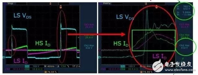
Figure 6
3.22 abnormal state analysis
Below we continue to analyze the potential risks to the LLC topology when the load changes drastically.
When the load changes rapidly, such as short circuit, dynamic load, etc., the key device MOSFET of the LLC circuit also faces challenges.
Generally, LLC will experience the following three states when the load changes. We call it hard-off, and in the right picture we can compare the difference in the internal MOSFET and CoolMOS internal carrier, and the risk to the MOSFET.

In timing 1, Q2 zero-voltage turn-on, reverse current through the MOSFET and body diode, then the secondary diode D2 open, D1 off.
- Traditional MOSFETs have electron currents flowing through the channel region, reducing the number of holes
- CoolMOS now has the same electron current as the conventional MOSFET through the channel, and the hole is reduced. The difference is that the P well structure of CoolMOS starts to build.

In timing 2, Q1 and Q2 are turned off simultaneously, and the reverse current flows through the MOSFET Q2 body diode.
When Q1 and Q2 are turned off, there is not much difference between the internal electron and hole path and flow direction for the conventional MOSFET and CoolMOS.
In timing 3, Q1 begins to turn on at this moment, because of the change of the load, the body diode of MOSFET Q2 needs very long time to recover in reverse at this moment. When the reverse recovery of the diode is not completed, the MOSFET Q2 is turned off hard. At this time, Q1 is turned on, and the voltage applied to the Q2 body diode causes a large current in the diode to trigger the BJT inside the MOSFET to cause an avalanche.
- Conventional MOSFETs draw out carriers at this time, and electrons are gathered around the PN junction. The hole current is congested at the edge of the PN junction.
- The electron current and the hole current of CoolMOS all go its own way. At this point, the hole current flows in the well-established P-well structure without electronic jamming.
In summary, when the LLC circuit is overloaded, short-circuited, and under dynamic load conditions, once the diode does not recover in time in the dead time, the resulting large combined current will trigger the MOSFET's internal BJT to disable the MOSFET.
Some CoolMOS adopts Super JucTIon structure. Under the condition that the MOSFET is hardly turned off, the carriers will be compounded along the vertically constructed P well, basically without lateral current, which greatly reduces the chance of triggering the BJT.
4. How to more easily implement ZVS
Through the above analysis, we can see that increasing the dead time of the MOSFET can provide enough diode reverse recovery time while reducing the risk of high dv/dt and di/dt to the LLC circuit. But is increasing dead time the only option? Below we further analyze how to reduce risk and improve system efficiency.
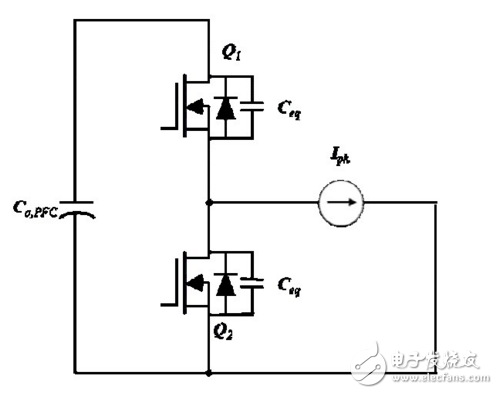
Figure 7
The initial current for the dead time for the LLC circuit is

The LLC can meet the ZVS must meet
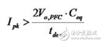
The minimum magnetizing inductance is

According to the above three equations, we can use the following three ways to let the LLC achieve ZVS.
First, increase Ipk.
Second, increase the dead time.
Third, reduce the equivalent capacitance Ceq, Coss.
From the above conditions, we can easily analyze. Increasing Ipk increases the size and cost of the inductor. Increasing the dead time will reduce the voltage during normal operation. The best choice is undoubtedly reducing the Coss, because the reduction does not need to make any adjustment to the circuit. It only needs to change to a Coss. Small MOSFET can be.
5 Conclusion
The LLC topology is widely used in a variety of switching power supplies, and this type of topology imposes new requirements on MOSFETs while improving efficiency. Unlike hard-switching topologies, the soft-switching LLC resonant topology not only has requirements for the on-resistance (on-state loss) and Qg (switching loss) of the MOSFET, but also how to effectively reduce the failure rate and improve the soft-switching performance. System reliability and lower system cost have higher requirements. CoolMOS has fast body diodes, low Coss, and breakdown voltages up to 650V, making the LLC topology switching power supply more efficient and reliable.
Cute and Small GPS Tracker for Pets
Features that already exist
âš« Tracking: It sends GPS (Location, speed) information to your application server with configurable report interval (moving or stationary).
âš« Geofence: It supports circle and polygon setting.
âš« SOS Button: Makes an SOS call or SMS message to a pre-configured phone.
âš« Mileage: Reports trip start, trip end and the mileage.
âš« 3-Axis Accelerometer: Using embedded accelerometer and carefully designed algorithm to detect the trip start/stop with accuracy.
âš« Battery Low Warning: When battery level is low, it will send low-battery alarm message.
âš« Cell-ID Based Location: Device reports cell-ID based location information if GPS signal is not available.
âš« Waterproof Case: IP65 waterproof.
âš« OTA (Over the Air): The device`s configuration, setting and firmware can be remotely upgraded.
âš« Mixed-mode: It will support 1-day-1-report mode, 1-hour check mode, power saving mode, super power saving mode, fix distance mode, fix interval mode and tracking mode to optimize the use of battery.
âš« WIFI-positioning: It will support WIFI feature for positioning.
âš« Multi-Platform: Customers can get device information through APP and web platform.
Other functions can be customized
Pets GPS Trackers,Animal GPS Tracker,Mini GPS Tracker,4G Pet GPS Trackers
eSky wireless Inc , https://www.eskygpsiot.com