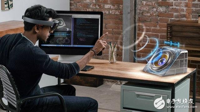
Microsoft unveiled its HoloLens Augmented Reality (AR) glasses and its dedicated accelerator, the Holographic Processing Unit (HPU) processing unit, at the IMEC Technology Forum in Brussels.
In late March of this year, Microsoft has begun shipping the developer version of HoloLens. The developer version of HoloLens was released, and the network was filled with various disassembly analysis, but so far no designers from this head-mounted display have made any comments.
"We have been publishing HoloLens for about 18 months and usually only emphasize the experience and software - this is the first time we are going to discuss the hardware," said Ilan Spillinger, vice president of development at Microsoft's HoloLens.

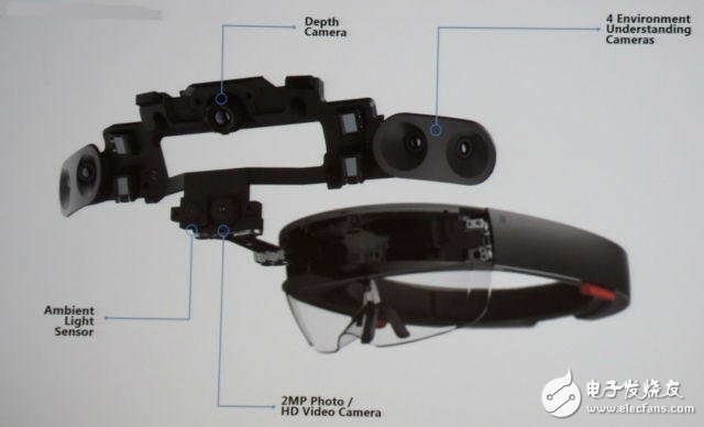
Microsoft's HoloLens head-mounted display includes four environmental sensors, a Kinect micro depth camera, and an inertial measurement unit (IMU). The HPU at its core is basically a data fusion sensor that captures input from a series of sensors on the HoloLens. At the same time, it speeds up the algorithm to track the user's environment, motion and gestures, and display holograms.
The 28nm HPU is basically a highly customizable DSP array design with less than 10W of power consumption. It includes multiple Tensilica DSP cores to optimize hundreds of HoloLens-specific instruction sets.
Each core is customized for a specific subset of functions and functions. In a architecture that sounds like Von Neumann, each core typically has its own unique memory cell organization that accelerates "a new algorithm that requires special local memory and a unique memory architecture, rather than the typical 1- 2-3 level cache," Spillinger explained.

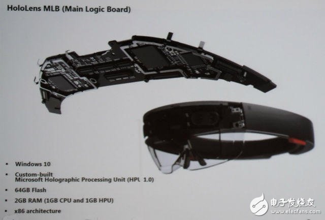
The HoloLens HPU is designed on a compact motherboard built for its headsets
The HoloLens headset is powered by the Intel 14nm Cherry Trail SoC and the embedded graphics core for Windows 10. It also has 64 Gb flash and 2 Gb of external memory on both sides of the motherboard, evenly distributed between its HPU and Cherry Trail SoC.
Spillinger did not reveal the development blueprint for this HPU, but said he has "seeed some new opportunities to implement the algorithm."
The HPU is also available for the new accelerators Google released for its data center last week, as well as a startup that is being developed by a startup.
Spillinger called on semiconductor engineers to prepare for the development of higher performance, lower power chips as soon as possible, helping them to create lighter, lower cost head-mounted displays with more sensors and features.
Ilan Spillinger began his career at Intel with Centrino, its first notebook-specific processor. Then he designed Infiniband and Power chips at IBM, and later helped Microsoft and Nintendo develop ASIC chips for Xbox 360 and Wii consoles.
Spillinger joined Microsoft at the end of 2007 and began developing Kinect. The program was later merged with other engineers' plans to develop augmented reality head-mounted displays, and the HoloLens program was born.
Complex sensor array

The HoloLens sensor array in the above image includes four environmental sensors for tracking head movements and controlling the gestures of the display. The depth sensor is a scaled-down version of Kinect that supports short-distance mode with gesture tracking of approximately 1 meter and long-distance mode within the imaging room. A 2 megapixel (2MPixel) high-resolution video camera is used to project images that the user sees.
Tin Spray Pcb,Tin Spraying Circuit Board,Multilayer Tin Sprayed Circuit Board,Pcb Spray Tin Board
Shenzheng Weifu Circuit Technology Co.Ld , https://www.viafoem.com