In Fig. 1, C1, V1~V4, C2 form a filter rectifier circuit, transformer T is a high frequency transformer, V5, R2, C11 constitute a protection circuit of power switch tube V7, and NF is a winding for supplying IC power. The single-ended output IC is UC3842, its 8 pin outputs 5V reference voltage, 2 pin is inverting input, 1 pin is amplifier output, 4 pin is oscillation capacitor C9, resistor R7 input terminal, 5 pin is grounding, 3 feet is The flow protection end, 6 feet for the single pulse output, and 7 pin for the power input. R6 and C7 form negative feedback. When the IC starts, the starting voltage is supplied by R1. After the circuit starts, the potential generated by NF is rectified and filtered by V6, C4 and C5 to supply the IC working voltage. R12 is an overcurrent protection sampling resistor, and V8 and C3 form a flyback rectification and filtering output circuit. R13 is the internal load, and V9~V12 and R14~R19 form the LED display circuit. In Figure 1, V5 and V6 select FR107, V8 selects FR154, and V7 selects K792.
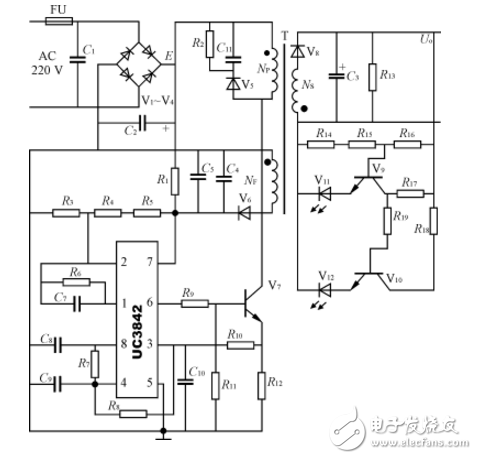
The circuit is charged with a switching power supply to reduce the weight and volume of the charger. The normal charging current of this charger circuit is 250MA, and the trickle charging current is 200MA.
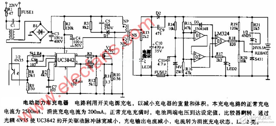
Commonly used electric car charger According to the circuit structure, there is a single-tube switching power supply with KA3842 driving FET, and the LM358 dual op amp is used to realize the three-stage charging mode. The principle is as follows:
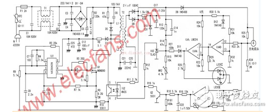
220v AC power is suppressed by T0 bidirectional filtering, D1 rectification is pulsating DC, and then C11 filtering forms a stable DC current of about 300V. U1 is a KA3842 pulse width modulation integrated circuit. The 5 pin is the negative pole of the power supply, the 7 pin is the positive pole of the power supply, the 6 pin is the pulse output, and the FET Q1 (K1358) 3 pin is the maximum current limit. Adjusting the resistance of R25 (2.5 ohm) can adjust the maximum current of the charger. . Pin 2 is voltage feedback and can adjust the output voltage of the charger. The 4-pin external oscillating resistor R1, and the oscillating capacitor C1.T1 are high-frequency pulse transformers, which have three functions. The first is to press the high voltage pulse into a low voltage pulse. The second is to isolate the high voltage to prevent electric shock. The third is to provide working power for the KA3842. D4 is a high-frequency rectifier tube (16A60V) C10 is a low-voltage filter capacitor, D5 is a 12V Zener diode, U3 (TL431) is a precision reference voltage source, with U2 (optocoupler 4N35) to automatically adjust the charger voltage. Adjust w2 (fine tuning resistor) to fine tune the charger voltage. D10 is the power indicator. D6 is the charging indicator. R27 is a current sampling resistor (0.1 ohm, 5w). Changing the resistance of W1 can adjust the high constant voltage of the charger.
Figure 2 is a switching power supply circuit composed of UC3842. The 220V mains is filtered by C1 and L1 to remove electromagnetic interference, and the negative temperature coefficient thermistor Rt1 is current-limited. After VC rectification and C2 filtering, the resistor R1 and the potentiometer RP1 are stepped down. After being added to the power supply terminal of UC3842 (7-pin), the startup voltage is provided for UC3842. After the circuit is started, the rectification and filtering voltage of the winding 34 of the transformer provides the normal working voltage for UC3842, and the voltage is applied by R3 and R4. The inverting input terminal of the error amplifier provides a negative feedback voltage for the UC3842. The rule is that the higher the voltage of the pin, the smaller the duty cycle of the driving pulse, thereby stabilizing the output voltage. The R6 and C8 externally connected to the 4th and 8th pins determine the oscillation frequency, and the maximum oscillation frequency can reach 500KHz. R5 and C6 are used to improve gain and frequency characteristics. The square wave signal outputted by the 6-pin is driven by the R7 and R8, and the MOSFEF power tube is driven. The energy of the primary winding 12 of the transformer is transmitted to the windings of the side, and after being rectified and filtered, the DC voltages of different values ​​are output for the load. Resistor R10 is used for current detection. It is filtered by R9 and C9 and sent to the 3rd pin of UC3842 to form a current feedback loop. Therefore, the power supply composed of UC3842 is a double closed-loop control system, and the voltage stability is very high. When the voltage of pin 3 of UC3842 is higher than 1V, the oscillator stops vibrating, and the protection power tube is not damaged by overcurrent.
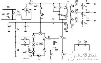
Figure 2 UC3842 switching power supply
Circuit debuggingThe debugging of this circuit needs to pay attention to: First, adjust the potentiometer RP1 to make the circuit start, the starting current is about 1mA; second, the DC voltage provided by the winding of the transformer 34 after starting the vibration should make the circuit work normally, the range of this voltage is about Between 11 and 17V; the third is to change R4 according to the value of the output voltage to determine the magnitude of the feedback amount; the fourth is to determine the size of the sense resistor R10 according to the protection requirements, usually R10 is 2W, 1Ω or less.
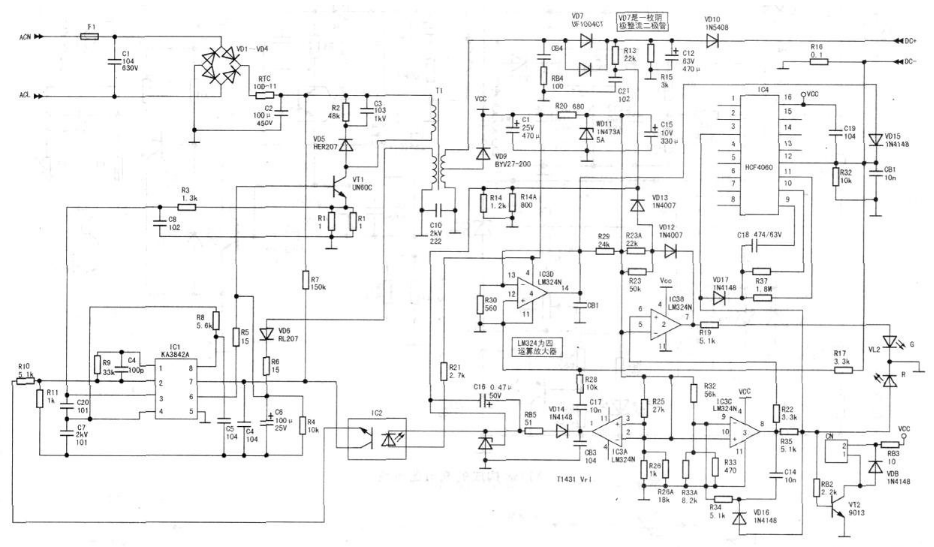
3842 charger circuit diagram (5)The following figure consists of a single-ended flyback pulse charger circuit consisting of KA3842+LM324+HCF4060.
The lithium ion battery charger circuit is composed of a power input conversion circuit, a constant current charging circuit, a constant voltage charging circuit, a working state indicating circuit and a battery voltage detecting control circuit, as shown in the figure.
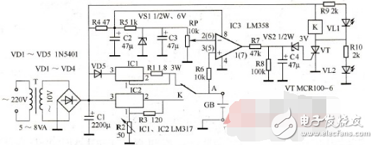
Figure Lithium-ion battery charger circuit using LM358 operational amplifier
The power input conversion circuit is composed of a power transformer T, a rectifier diode VD1 - VD4 and a filter capacitor C1; the constant current charging circuit is composed of a diode VD5, a three-terminal voltage regulator integrated circuit IC1 and a resistor R1; the constant voltage charging circuit is integrated by a three-terminal voltage regulator Circuit IC2 and resistors R2, R3; battery voltage detection control circuit consists of resistors R4 ~ R8, capacitors C2 ~ C4, potentiometer RP, Zener diode VS1, VS2, operational amplifier IC3, thyristor VT and relay K; The circuit consists of resistors R9, R10 and LEDs VL1, VL2.
After the AC 220V voltage is stepped down by T, VD1~VD4 is rectified and C1 is filtered, the battery GB is subjected to constant current charging through the constant current charging circuit and the normally closed contact of K. When the voltage of the battery rises to 4.2V, IC3 outputs a high level, VT is triggered by VS2 to conduct, K is energized, its normally closed contact end is disconnected, normally open contact is turned on, after rectification and filtering The DC voltage is subjected to constant voltage charging by the constant voltage charging circuit.
In the first stage of constant current charging, VL2 lights up; in the second stage of constant voltage charging, VL1 lights up.
After the circuit is installed, disconnect R7, connect the power supply, and adjust the resistance of the RP so that the center tap voltage is 4.2V. Connect a 47Ω dummy load between the output of IC2 and ground, and adjust the resistance of R2 so that the voltage of pin 2 of IC2 is 4.2V. Disconnect the power supply and the dummy load, connect the R7 and the battery to be charged GB, and then turn on the power to charge. Monitor the voltage across the GB to ensure that the voltage across the GB reaches 4.2V and the K is energized, otherwise the resistance of the RP should be fine-tuned.
Wireless Vacuum Cleaner,Best Wireless Vacuum Cleaner,Wireless Car Vacuum Cleaner,Best Vacuum Cleaner Wireless
Ningbo ATAP Electric Appliance Co.,Ltd , https://www.atap-airfryer.com