The voltage doubler rectifier circuit is based on the energy storage function of the capacitors, and together form a voltage doubler rectifier circuit, which can "convert" a higher DC voltage with a lower AC voltage and a rectifier diode and a capacitor with lower withstand voltage. The withstand voltage of the rectifying element can also be relatively low, so such a rectifying circuit is particularly suitable for applications requiring high voltage and low current.
working principleThe voltage doubler rectification uses the rectification and guiding action of the diodes to store the voltages on the respective capacitors, and then serially connect them according to the principle of polarity addition, and output a high voltage higher than the input voltage. The figure below is a 2x voltage rectifier circuit.

In the above figure, R1 and R2 are current limiting resistors, and RL is the converted value of the load. First, in the first half of the week E2, C1 charges C1 to the peak E2m of E2, and the voltage on the second half of C1 and the power supply voltage are added to charge C2 to C2 to 2E2m. Of course, the voltage on the capacitor for several cycles cannot be charged to such a high level, but after several cycles, the voltage on C2 can gradually stabilize at about 2E2m, which is the principle of 2 times voltage rectification.
DC double voltage rectification circuit diagram (1)Double voltage rectification is a rectification method that utilizes the charge and discharge effect of a capacitor. The basic circuit is a double voltage rectification circuit, and the multiplying voltage rectification circuit is a generalization of a double voltage circuit. The following describes the principle of double voltage and multi-voltage rectifier circuits:
1) The working principle of double voltage rectifier circuit
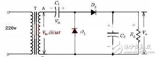
When Vm is in the negative half cycle, the voltage polarity is as shown in the figure below (left), D1 is turned on, D2 is turned off; C1 is charged, current
The direction and the voltage polarity on C1 are shown in the figure below (left), and the maximum voltage of C1 can reach Vm.
When Vm is in the positive half cycle, the voltage polarity is as shown in the figure below (right), D2 is on, D1 is off; C2 is charged, the current direction and the voltage polarity on C2 are as shown in the figure below (right), due to the storage of charge, The output voltage (ie, the voltage on C2) is twice the voltage of the secondary side of the transformer, and the maximum value of the C2 voltage is up to 2Vm. It should be noted that the voltage of C2 cannot be charged to 2Vm in one half cycle, and it must gradually approach 2Vm after several cycles.

When several half-wave voltage doubler rectifier circuits composed of diodes and capacitors are connected in series in several stages, the AC voltage is charged and discharged in series and parallel to the capacitors C1 to Cn through the diodes D1 to Dn every half cycle. The AC input voltage can be used to obtain several times the DC output voltage of a single-stage half-wave voltage doubler rectifier circuit.

The working process is: first, during the negative half cycle of the alternating current, the alternating current source charges C1 through D1, then the alternating current source and the voltage on C1 are added in the positive half cycle, and the capacitor C2 is charged through D2, and the charged voltage is the charging voltage of the capacitor C1. Twice. Next, in the negative half cycle, in addition to the power supply charging the capacitor C1 via D1, the AC power supply is superimposed with the voltage on C2 via D3 to charge C3, C1, and the charging voltage on C3 is twice that on C1. During the positive half cycle, the AC power supply is superimposed with the voltage on C1. In addition to charging capacitor C2 via D2, it also superimposes the voltage on C1 and C3 via D4 to charge capacitors C4 and C2. The voltage charged on C4 is capacitor C1. Double the voltage. By analogy, it can be seen that the output DC voltage is related to the number of stages of the half-wave voltage doubler rectifier circuit. The figure is connected in series with a three-stage half-wave voltage doubler rectifier circuit. The charging voltages on C2, C4 and C6 are twice the charging voltage on C1. After three capacitors are connected in series, the charging voltage is six times the charging voltage on C1.
DC double voltage rectification circuit diagram (3)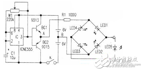
Circuit working principle
The IC is connected to a self-excited multi-resonant circuit whose oscillation frequency is controlled by C1 and W4. The oscillating signal output from the IC3 pin controls BG1 and BG2 to be turned on in turn, so that the potential at point A becomes high and low alternating current with respect to point B. When the lC3 pin outputs a low level, BG2 is turned on, and BG1 is turned off, so that point A is low level, point B is high level, and current flows through B→LED2→LED5→LED4→A. At this time, LED2, LED5, and LED4 all emit light. When the IC3 pin outputs a high potential, BG1 is turned on, BG2 is turned off, point A is high, and point B is low. At this time, the current flows through A→LEDI→LED5→LED3→B, and LED1, LED5 and LED3 all emit light, so that the whole circuit simulates the bridge rectification process. In the circuit, LED5 is used to demonstrate the positive and negative polarity of the output of the bridge rectifier circuit.
Component selection and production
The IC selects the time base circuit NE555 or HA17555. C1 and W1 can be selected according to the actual situation to meet different needs. Five LEDs can be selected for high brightness, but LED 5 is preferably different from the other four LFD colors. The battery can be used with two 6V stacked batteries. The whole circuit can be mounted on a large plywood. Five LEDs are mounted on the front side of the board, and the bridge rectification circuit is drawn at the corresponding position. It is worth noting that the value of C1 should be such that the LED has obvious resolution when it is turned on and off in turn. Adjusting Wl can change the oscillation frequency, that is, the frequency of the alternating current is equivalently changed. If a voltmeter is connected to two points A and B, in the static state, the pointer is pointed at the middle reticle position. In this way, as the BGI and BG2 turn on and the pointer can swing left and right, it can be more intuitively demonstrated that "the direction of the alternating current is constantly changing."
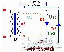
DC double voltage rectification circuit diagram (4)The circuit consists of a transformer B, two rectifier diodes D1, D2 and two capacitors C1, C2.
The working principle is as follows: when the double voltage rectifier circuit e2 is in the positive half cycle (upper positive and negative), the diode D1 is turned on, D2 is turned off, the current is charged to C1 through D1, and the voltage on the capacitor C1 is charged to the peak close to e2 √ 2E2 And remains basically unchanged. When e2 is negative half cycle (upper negative and positive), diode D2 is turned on and D1 is turned off. At this time, the voltage Uc1=√2E2 on C1 is added in series with the power supply voltage e2, and the current charges the capacitor C2 via D2, and the charging voltage Uc2=e2 peak + √2E2 ≈ 2√2E2. Repeatedly charged, the voltage on C2 is basically 2√2E2. Its value is twice the voltage of the transformer's power stage, so it is called a double voltage rectifier circuit.
In an actual circuit, the voltage across the load is approximately equal to 2X√2E2. The highest reverse voltage experienced by rectifier diodes D1 and D2 is 2X√2E2. The DC voltage Uc1 on the capacitor is √2E2 and Uc2=2√2E2. Circuits and selection components can be designed accordingly.
On the basis of the double voltage rectification circuit, a rectifier diode D3 and a filter capacitor C3 are added to form a triple voltage rectifier circuit. The working principle of the triple voltage rectifier circuit is: in the first half of e2 and the second half of the same double voltage rectifier circuit, i.e. the voltage across C1 is charged to near √2E2, the voltage across C2 is charged to near 2√2E2. When the third half is over, D1 and D3 are turned on, D2 is turned off, the current is charged by C1 except D1, and C3 is charged by D3. The charging voltage Uc3=e2 peak + Uc2-Uc1≈2√2E2 on C3 On the RFZ, the DC voltage Usc=Uc1i+Uc3≈3√2E2 can be output to realize triple voltage rectification. Triple voltage rectifier circuit In the actual circuit, the voltage on the load Ufz ≈ 3x1.4E2 rectifier diode D3 is subjected to the highest reverse voltage is also the DC voltage on the capacitor is 3 √ 2 E2.
In this way, by adding multiple diodes and the same number of capacitors, it is possible to form a multiple voltage rectifier circuit, see the triple voltage rectifier circuit. When n is an odd number, the output voltage is taken out from the upper end: when n is an even number, the output voltage is taken out from the lower end.
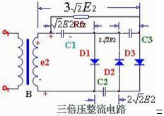
It must be stated that the voltage doubler rectifier circuit can only work when the load is light (ie, Rfz is large and the output current is small), otherwise the output voltage will decrease. The higher the voltage doubler, the more obvious the increase in output voltage due to the increase in load current.
The diode used in the voltage doubler rectifier circuit should have a maximum reverse voltage greater than. A high-voltage silicon rectifier stack is available, and its series model is 2DL. For example, 2DL2/0.2 means that the highest reverse voltage is 2 kV, and the average rectified current is 200 mA. The capacitor used in the voltage doubler rectifier circuit has a relatively small capacity and does not require an electrolytic capacitor. The capacitor's withstand voltage is greater than 1.5x, which is safe and reliable in use.
DC double voltage rectification circuit diagram (6)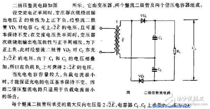
The KSPOWER brand CLASS 2 power supply provides the complete Class 2 power transformer solutions covering a output power ranging from 4.2 Watts to 100 Watts and beyond with output voltages and currents ranging from 4.2V DC to 48V DC, 100ma to 5000ma LED driver. The class 2 power adaptor is PC materials with IP20 rated environment protection for indoor LED lighting. The class 2 led Power Supplies is UL1310 safety standard designed and offers 3 years after-sale customer service and both UL/cUL, Class 2, FCC CE RoHS Listed safety certificate and compact style enclosures. The led lamp driver provides various connection types:desktop, wall mount, cord to cord three types, safety protections for short circuit, over load, over voltage and over temperature. The ac to dc power supply accepts various dc connector size for LED lights. If you are looking for UL cUL Class 2 AC to DC LED lighting power supply for your LED strip signs applications, KSPOWER can help you, welcome to contact and inquiry!
Led Lamp Driver,Led Power Supplies,universal power supply,oem power supply,ac to dc power supply
Shenzhenshi Zhenhuan Electronic Co., Ltd , https://www.szzhpower.com