In recent years, the global supply of silicon wafers has been insufficient, resulting in orders for 8-inch and 12-inch silicon wafers having reached the first half of 2019 and the end of the year. At present, a number of domestic silicon wafer projects have begun, and it is expected to be able to break the import dependence and have sufficient capacity to meet market demand.
Knowledge point 1: What is a silicon wafer?
The silicon wafer is purified by silicon (99.999%), and then the pure silicon is made into a long silicon ingot, which becomes the material of the quartz semiconductor for manufacturing the integrated circuit. After photolithography, grinding, polishing, slicing, etc., the polysilicon is used. The monocrystalline silicon ingot is melted and then cut into a thin wafer.
1. Purification. Divided into two stages, the first step is metallurgical purification. This process is mainly to add carbon to convert silicon oxide into silicon with a purity of 98% or more by oxidation-reduction. Most metals are refined, such as metals such as iron or copper, in such a way that metals of sufficient purity are obtained. However, 98% is still insufficient for chip manufacturing and still needs further improvement. Therefore, the Siemens process will be further used for purification, and thus, high-purity polycrystalline silicon required for the semiconductor process will be obtained.

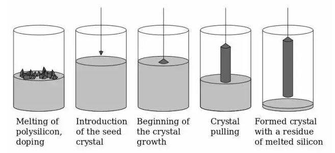
Figure: Silicon column manufacturing process
2, pull crystal. First, the high-purity polycrystalline silicon obtained above is melted to form liquid silicon. Thereafter, the single crystal silicon seed is brought into contact with the surface of the liquid, and is slowly pulled up while rotating. As for why a single crystal silicon is needed, it is because the arrangement of silicon atoms is the same as that of people, and it will be necessary to arrange the heads so that later people can arrange them correctly. The silicon species is an important leader, so that later atoms know how to line up. Finally, after the silicon atoms leaving the liquid surface are solidified, the aligned single crystal silicon columns are completed.

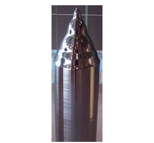
Figure: Monocrystalline silicon column
3. Cut into pieces. However, a whole silicon column cannot be made into a substrate made of a chip. In order to produce a piece of silicon wafer, the silicon crystal column is then cut into a wafer by a diamond knife, and the wafer can be formed into a wafer by polishing. Fabricate the required silicon wafers.

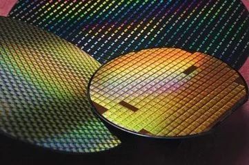
Figure: Silicon wafers are long like this
What is 6 inch, 8 inch, 12 inch?
Refers to the diameter of the resulting crystal column after the surface has been treated and cut into thin discs. The larger the size, the higher the speed and temperature requirements of the crystal pull, so it is more difficult to make high quality 12-inch wafers than the 8-inch wafer.
Knowledge point 2: Which manufacturers produce silicon wafers?
Silicon wafers for integrated circuits are cutting-edge high-tech products with extremely high manufacturing technology. Only about 10 companies in the world can manufacture them, and the top five companies have a market share of 90%. The world's first two integrated silicon wafer manufacturers are Shin-Etsu and SUMCO, which account for more than 60% of the world's total; the two companies produce large-size silicon wafers (200mm and 300mm) that account for 70% of the world's total. Above %, an absolute monopoly and extremely high technical barriers are formed.
Global wafer manufacturers include Shin-Etsu, Sumco, Global Wafer, Siltronic, LG Siltron, Soitec, and Wafer Works ), Finland's Okmetic, Taiwan's Episil.
In August 2017, SUMCO announced that it had invested approximately US$397 million to increase its production of its Imari plant, which was the first large-scale increase in production in the past decade. It is expected to increase the monthly production capacity of 12-inch silicon wafers by 110,000 in the first half of 2019.
Global wafers are deployed in Taiwan, China, Japan, Europe and the United States. The company has partnered with Japan's semiconductor equipment factory Ferrotec to build a Shanghai 8-inch silicon wafer fab, with an initial monthly production capacity of about 100,000. At the same time, the two sides have also negotiated to build an 8-inch factory in Hangzhou. The initial plan is to start production at the end of 2019.
Global Wafer is a subsidiary of Sino-US Silicon Crystal. In 2012, it acquired the semiconductor wafer business of CovalentMaterials (now CoorsTek), formerly Toshiba Ceramics, and expanded its business scope. After the acquisition of the world's fourth largest semiconductor silicon wafer manufacturing and supplier SunEdisonSemiconductor became the third largest silicon wafer supplier.
Siltronic, the world's fourth-largest silicon wafer manufacturer, is headquartered in Munich, Germany. The data shows that the company has a 150/200/300mm production line in Germany, a 200mm wafer fab in the US, and 200 and 300mm production lines in Singapore. .
LG Siltron is a specialized company that manufactures silicon wafers for semiconductor chip base materials. However, the SK Group acquired a 51% stake in LG Siltron in January 2017 to break into the semiconductor materials and parts sector.
On March 21, 2018, Xu Jianhua, chairman of Jiajing, said that the customer demand for Jiajing is very strong. It is difficult to meet the single-track. The orders for vehicles, mining and data centers are particularly strong, and some customers even require signing. Long-term to ensure production capacity. Jiajing expanded its production capacity at the beginning of this year. The new production capacity will continue to be produced in the second quarter. Subsequent expansion will also focus on niche products.
What are the domestic silicon wafer projects?
At present, silicon projects have been started in China, including Shanghai Xinsheng, Chongqing Super Silicon, Ningxia Yinhe, Zhejiang Jinruiqi, Zhengzhou Hejing, and Xi'an High-tech Zone Project. The total investment scale is over RMB 52 billion, and the planned monthly capacity of 12-inch wafers has reached 1.2 million.
Xinsheng Semiconductor is one of the world's leading 12-inch large silicon wafer manufacturers, focusing on the manufacture of 300mm silicon wafers. In 2017, the company will start trial production and provide test films to various customers. In the past six months, it has produced tens of thousands of pieces per month. Currently, the first phase of the construction of 100,000 wafers per month is underway. It is expected to be completed within this year, and in the second half of this year, the next phase will start with 200,000 silicon per month. The construction of the film capacity is expected to be completed in 2019.
On March 18, 2018, the large-scale semiconductor wafer project of Ningxia Yinhe Semiconductor Technology Co., Ltd. with a total investment of 1.6 billion yuan was started in Yinchuan Economic and Technological Development Zone. After the project is completed, it can produce 4.2 million 8-inch semiconductor-grade monocrystalline silicon wafers and 2.4 million 12-inch semiconductor-grade monocrystalline silicon wafers per year.
The latest announcement from Tianjin Zhonghuan Semiconductor shows that the company has achieved mass production of 8-inch Czochralski crystals in Czochralski single crystals, and in the first quarter of 2018, it has achieved trial production of 12-inch Czochralski single crystal samples. In the semiconductor area melting single crystal and polishing sheet, the production capacity of the 8-inch semiconductor polishing sheet project has been released. In March 2018, the 8-inch polishing sheet capacity has reached 100,000 pieces/month, and the project is expected to be completed in October 2018.
After-production capacity will reach 300,000 pieces/month, achieving the largest market share in China, and establishing a 12-inch polished film test line. It is expected to achieve a production capacity of 20,000 pieces per month by the end of 2018. In the industrialization of large-diameter polished sheets in Jiangsu, the company expects equipment to be commissioned in the fourth quarter of 2018. After the completion of the project investment, it is estimated that in 2022, the production capacity of 8 inch polishing pad will be 750,000 pieces/month, and the production capacity of 12-inch polishing piece will be 600,000 pieces/month.
Chongqing Super Silicon Semiconductor started construction in May 2014 and put into trial production in April 2016. In May 2016, the first IC-grade 8-inch monocrystalline silicon rod was successfully pulled out; in September 2016, the first IC-grade 12-inch single-crystal silicon rod was successfully pulled out; the first batch of IC-class monocrystalline silicon in October 2016 Successfully rolled off the line, indicating that the project of 300mm (including 200mm) single crystal silicon crystal growth and polishing silicon wafer and extension product (Phase I) for the very large scale integrated circuit was officially completed, and the product off-line ceremony was held; 2017 1 The first batch of 200mm silicon wafer products were shipped from the factory on the 20th of the month. After production, it will achieve an annual production capacity of 6 million pieces of 8-inch silicon wafers and 600,000 pieces of 12-inch silicon wafers.
In January 2017, Jinrui Technology (Zhangzhou) Co., Ltd. held a groundbreaking ceremony with a total investment of 5 billion yuan, and built a project scale of 400,000 8-inch wafers per month and 100,000 wafers per month. The project plan is gradually implemented in three phases. The total investment of the first phase is about 700 million yuan. The construction period is from 2017 to 2019. The land is 100 mu. It is planned to build 100,000 8-inch silicon epitaxial wafer projects in 2017. The total investment of the second and third phases is 4.3 billion yuan. Mu will form a production line with a monthly production capacity of 300,000 8-inch wafer projects and a monthly production capacity of 100,000 wafers for 12-inch wafers.
On July 27, 2017, Zhengzhou Hejing Silicon Materials Co., Ltd. held an annual production meeting of 2.4 million pieces of 200mm silicon single crystal polishing sheet production project mobilization meeting. The project plans a total investment of 5.3 billion yuan, covering an area of ​​153 acres, mainly to build 200 mm, 300 mm silicon substrate and epitaxial wafer production base. The project will be implemented in two phases. The first phase will have a capacity of 200,000 pieces of silicon substrate 200,000 pieces per month, and the second stage will have a capacity of 300,000 pieces of silicon material, 250,000 pieces per month, and 90,000 pieces of epitaxial wafers.
On December 9, 2017, the signing ceremony of the Siswei Silicon Industry Base project was held in Xi'an. Xi'an High-tech Zone and Beijing Core Dynamics Co., Ltd. and Beijing Siswei Company signed a letter of intent for investment cooperation in the silicon industry base project. According to the letter of intent, the total investment of the project is more than 10 billion yuan, which is planned and promoted by the Beijing Weisiwei Company of Beijing Core Dynamics.
Knowledge Point 3: Interpretation of Supply and Demand
According to Gartner's forecast, the global wafer market will reach about 11 billion US dollars by 2020. At present, the global silicon wafer supply, the monthly capacity of 12-inch silicon wafers is about 550-5.6 million. At present, the country does not have the production capacity of 12-inch silicon wafers, and has always relied on imports. The current domestic total demand is about 450,000 pieces/month. It is estimated that by 2020, the monthly demand for 12-inch silicon wafers in China will be 800-100 million pieces.
It is understood that the monthly capacity of 12-inch silicon wafers in domestic planning has reached 1.2 million pieces. If it goes smoothly, then the capacity can meet the needs of itself. In addition, industry insiders said that if the domestic 8-inch project can achieve mass production targets, there may be overcapacity
Insulated Power Cable,Bimetallic Crimp Lugs Cable,Pvc Copper Cable,Cable With Copper Tube Terminal
Taixing Longyi Terminals Co.,Ltd. , https://www.longyicopperlugs.com