1 Main features of DaVinci technology
The DaVinci platform is a typical shared storage-based embedded multiprocessing (ARM, DSP, VICP, video front-end and back-end, etc.) environment. The key technology supported is the on-chip implementation of multi-channel switching center resources (Switch Central Resources , SCR). Based on the on-chip SCR, the DaVinci platform has formed a typical C / S architecture between on-chip multi-processors: a powerful computing DSP can be used as a server to provide real-time computing services for algorithms; ARM9 with JAVA processing capability realizes the network , Hard disk audio and video I / O and other user interfaces. On the DaVinci platform, American TI has designed a system framework for audio and video codec (Codec) multimedia applications. It provides a rich system program interface SPI, application program interface API, and more than 1,000 kinds of video, image, voice and audio. Streaming media algorithm component. They and the operating system and middleware constitute most of the content of an application system. The application system development team only needs to encapsulate them into a running package to get high availability and high reliability products.
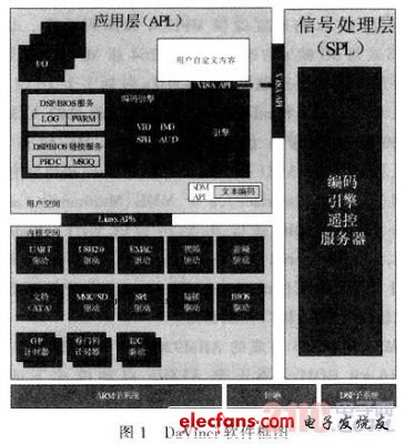
The biggest feature of the DaVinci platform is the SOC chip based on DSP and ARM, and related software, as shown in Figure 1.

For the DaVinci platform, the hardware gives strong support to the dual-core architecture, using DPS / BIOS on the DSP side to support the operation of audio / video algorithms, and MontaVistaLinux (MV) on the ARM side to support the management of its peripherals. For the data cross between ARM and DSP, it is managed with Codec Engine and Codec Server. The advanced nature of the DaVinci platform is undoubtedly the best choice for development platforms for high-end audio / video systems.
2 Introduction of TMS320DM365
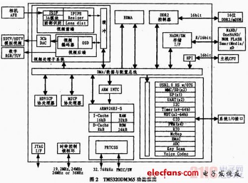
TI's TMS320DM365 is a high-performance chip for multimedia technology applications. The functional block diagram of TM320DM365 is shown in Figure 2.

In the core, TMS320DM365 integrates ARM926EJ-SH264 coprocessor (HDVICP), MPEG4 / JPEG coprocessor (MJCP), can provide H.264 codec function in 1080p format and 10 frames / s, and 1080p format and 24 frames / s speed provides MPEG4 codec function, as well as H.264 or MPEG4 codec function in 720p format and 30 frames / s speed. In terms of storage, the extended memory interface EMIFs include a 16-bit DDR2 and mDDR with 256 M address space, and a 16 / 8-bit AEMIF. The expandable types are 8 / 16-bit NAND Flash, 16Mb NOR Flash, SRAM, 16-bit OneNAND, etc. Other peripheral expansion controllers also include 16-bit HPI (Host-Port Interface), 2 MMC (MulTImedia Card) / SD (Secure Digital) / SDIO interfaces, 1 16-bit WDT (Watch DogTImer), 5 SPI (Serial Port Interface) interface, each of which has two chip selects, one master / slave I2C (Inter-Integrated Circuit) bus controller, and one supports 2.0USB OTG interface controller.
The TMS320DM365 integrated ARM926EJ-S processor includes 32 kBRAM, 16 kB ROM (for ARMbootloader in non-AEMIF boot mode), 16 kB instruction cache, 8 kB data cache, CP15 and MMU. CP15 is used to configure and control the instruction, data cache, MMU and other ARM subsystems. MMU uses a unified TLB to cache the information stored in the page table and provides virtual memory for operating systems like Linux, WindowsCE, ultron, and ThreadX. The processor's write buffer data capacity is up to 17 kB, making it possible to greatly improve the performance of the core.
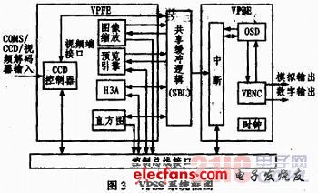
The video processing subsystem (VPSS) in the TMS320DM365 consists of two interfaces, a video front-end (VPFE) input interface for video capture and a video back-end (VPBE) output interface for image display. Figure 3 is a block diagram of the video processing subsystem system.

The VPFE module is mainly used to capture video signals, and can also directly input existing video signals from the front end. The VPFE input interface is composed of a CCD controller (CCDC), a pre-processor, a columnar module, an automatic exposure / white balance / focus module (H3A) and a register. CCDC can be connected to a video decoder, CMOS sensor or charge-coupled device; the pre-processor is a real-time image processor that converts the original image from CMOS or CCD from RGB to YUV422 encoding; the columnar module and H3A module are based on The hardware operation of the original image information.
The VPBE output interface consists of an OSD engine and a video encoder. The OSD engine can display two sets of independent video windows or two sets of independent OSD windows, and can also be displayed in the form of 2 video windows, 1 OSD window, and one property window. OSD is used to superimpose volume, icon and other bitmaps or image information on video images. The video encoding module provides digital output and analog output. Digital output supports 24bitRGB888 format, 8 / 16bit BT.656, and CCIT.601 output with independent horizontal and vertical synchronization functions; analog output supports four 10-bit DACs, all working at 54 MHz, supporting composite NTSC / PAL, S terminal and Component video.
Microstepping is a method of controlling stepper motors, typically used to achieve higher resolution or smoother motion at low speeds.
Micro stepper motor divides each full step into smaller steps to help smooth out the motor`s rotation, especially at slow speeds.
Microstepping is achieved by using pulse-width modulated (PWM) voltage to control current to the motor windings. The driver sends two voltage sine waves, 90 degrees out of phase, to the motor windings. While current increases in one winding, it decreases in the other winding. This gradual transfer of current results in smoother motion and more consistent torque production than full- or half-step control.
Micro stepper motor,Micro linear stepper motor,Micro stepping stepper motor
Shenzhen Maintex Intelligent Control Co., Ltd. , https://www.maintexmotor.com