Power supply design buffer forward converter
Calculating how much capacitance and resistance to add is a challenging task. Here's a quick way to solve this problem.
Figure 1 shows the power level of the forward converter. The converter is operated by a transformer that couples the input voltage to the secondary circuit and the secondary circuit completes the rectification and filtering of the input voltage. The reflected main voltage and transformer leakage inductance form a low-impedance circuit. When D2 is forced off by a resistor like this, a snubber is usually required. D2 can be a silicon pn diode that has a reverse recovery charge function that must be depleted before it is turned off. This loads up excess current in the leakage inductance, resulting in high frequency ringing and excessive diode voltage. Schottky diodes and synchronous rectifiers have similar conditions. The former is due to their large junction capacitance, and the latter due to their turn-off delay time.
Figure 1 Leakage inductance delays D2 off
Figure 2 shows some of the circuit waveforms. The top trace is the Q1 drain voltage, the middle trace is the voltage at the D1 and D2 junctions, and the bottom trace is the current through D1. In the top trace, you can see that when Q1 opens, its drain voltage is reduced below the input voltage, which causes the diode D1 current to increase. If D2 does not have a reverse recovery charge function, the junction voltage will rise when the D1 current is equal to the output current. Since D2 has a reverse recovery charging function, the D1 current will further increase, which will start to consume the charge. Once the charge is depleted, the diode is turned off, causing the increased junction voltage to increase further. Note that the current will increase until the junction voltage equals the reflected input voltage because there is a positive voltage across the leakage inductance. As the current increases, this current will charge the parasitic capacitance and cause greater ringing and loss in the circuit.
Figure 2 D2 can cause excessive ringing when D2 is off
These ringing waveforms may be unacceptable because they can cause EMI problems or cause unacceptable voltage stress on the diodes. The RC buffer across D2 can greatly reduce ringing while hardly affecting efficiency. You can use the following equation to calculate the ringing frequency (see Equation 1):
Equation 1:
But how do you know the values ​​of L and C in the circuit? The trick is to reduce the ringing frequency by adding a capacitor with a known capacitance across D2, and you get two equations and two unknowns. If you add a capacitor that can just halve the ringing frequency, it will make it easier to find the above values. To reduce the half frequency, you need a total capacitance that is 4 times the parasitic capacitance you used initially. Then, as long as the added capacitance is divided by 3, the parasitic capacitance can be obtained. Figure 3 shows the waveform of a 470 pF capacitor across D2 when the frequency is half of the original ringing frequency. Therefore, the circuit has a parasitic capacitance of about 150 pF. Note that the addition of a capacitor only has little effect on the amplitude of the ringing, and the circuit also needs some resistance to damp the ringing. This is another reason why the capacitance factor 3 is a good place to start. If you choose the right resistor, then this resistor can provide excellent damping while minimizing the impact on efficiency. The optimum value of the damping resistor is almost the typical resistance of the parasitic element (see Equation 2).
Equation 2: Information Source: http://tede.cn
Figure 3 Doubles the ringing frequency to complete the parasitic calculation
Equation 3:
Once the calculations are complete, you need to determine if the circuit can withstand the losses in the buffer. If not, you need to make a trade-off between ringing and snubber losses. For details on how to choose the best damping resistor, see Figure 3 Power Supply > Power Supply Design Tip 4 on page 3.
Figure 4 Choosing an Appropriate Buffer Resistor Eliminate Ringing altogether
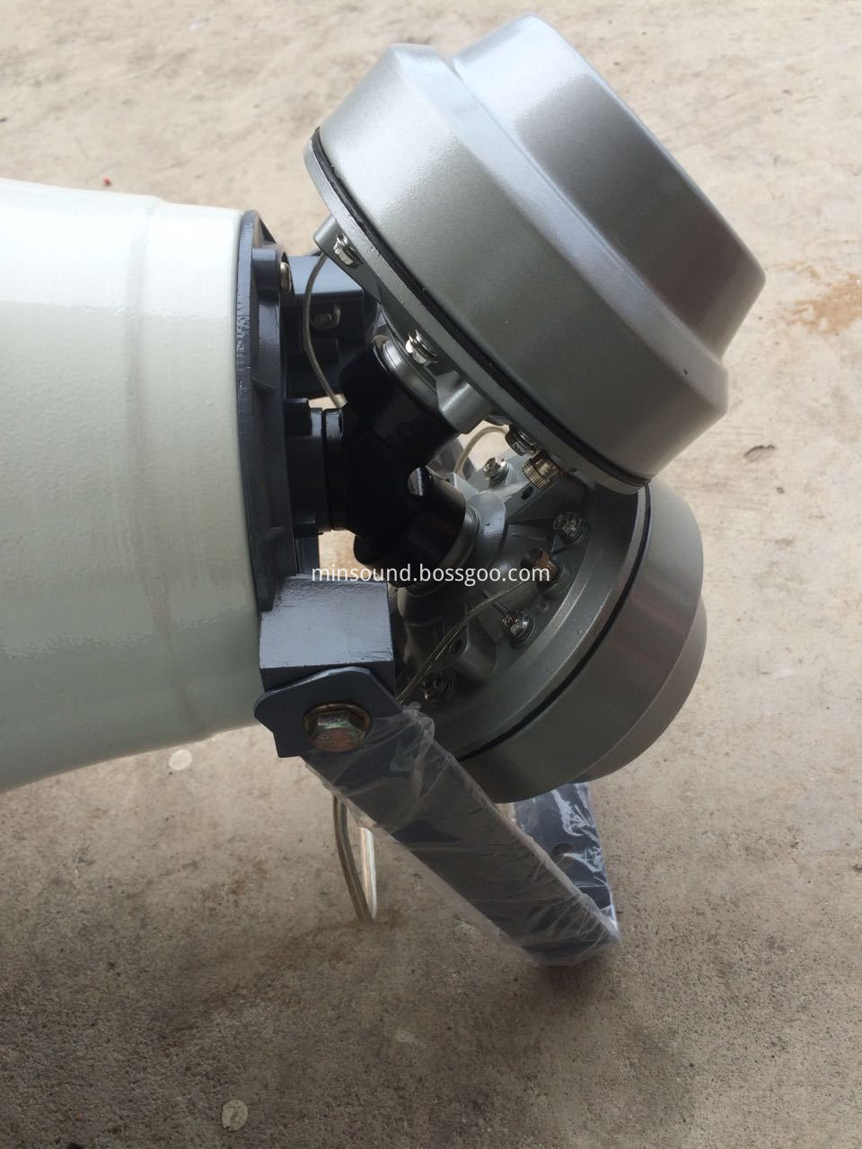
This series can connect two Driver Unit,so it is more powerful, not easy to burn out ,this driver unit connector is made of all-aluminum material, firm and wear-resistant, anti-freeze and anti-pressure, durable, , easy to install, long service life is also its strong point.it can also be used for HS200-02.
Driver Unit connector,Driver Unit Y Adapter,Compression Driver Y Adapter,Aluminum Y Adapter
Taixing Minsheng Electronic Co.,Ltd. , https://www.msloudspeaker.com