Circuit function and advantage
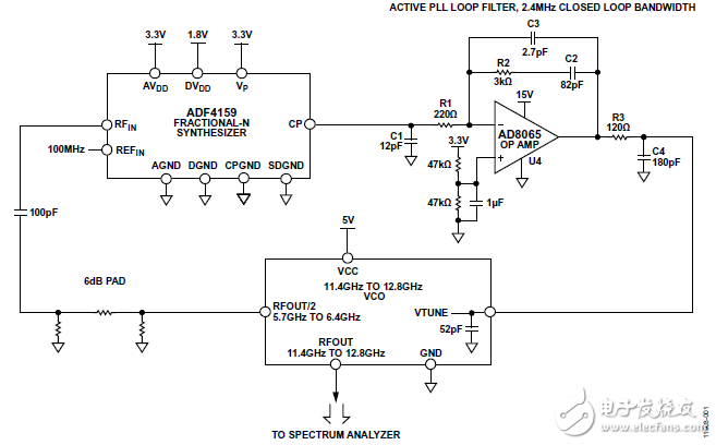
The PLL circuit shown in Figure 1 uses a 13 GHz fractional-N frequency synthesizer, a wideband active loop filter, and a VCO. The 200 MHz frequency hopping phase settling time within 5° is less than 5 μs.
This performance is achieved with an active loop filter with a bandwidth of 2.4 MHz. Since the ADF4159 phase frequency detector (PFD) has a maximum frequency of 110 MHz and the AD8065 op amp has a high gain bandwidth product of 145 MHz, this wide bandwidth loop filter performance is available.
The AD8065 op amp used in the active filter is capable of operating from a 24 V supply voltage, allowing control of most wideband VCOs with tuning voltages from 0 V to 18 V.

Figure 1. Functional block diagram of the ADF4159, active loop filter AD8065, and 11.4 GHz to 12.8 GHz VCO (schematic diagram: all connections and decoupling not shown)
Circuit description
In PLL and VCO frequency synthesis systems, obtaining a frequency and phase setup time of less than 5 μs requires an extremely wide loop bandwidth. The loop bandwidth (LBW) defines the speed of the control loop. A wider LBW allows for faster settling times, but at the expense of phase noise and the attenuation of spurious signals. The circuit shown in Figure 1 locks the ADF4159 to the RFOUT/2 signal (~6 GHz) of the 12 GHz VCO (MACOM MAOC-009269). However, a VCO with RFOUT/2 signal and up to 24 GHz can be used with the ADF4159 because it supports a maximum RF input of 13 GHz.
ADF4159 fractional-N frequency synthesizer
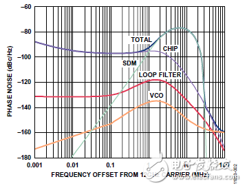
In the fractional-N architecture PLL, from  The noise of the modulator (SDM) peaks at half the PFD frequency (fPFD). For example, if the PFD frequency of a fractional-N PLL is 32 MHz, the unfiltered SDM noise peaks at 16 MHz. SDM noise makes the loop unstable, causing the PLL to fail to lock. Figure 2 shows the simulated phase noise curve for this condition.

Figure 2. Phase noise curve at 12 GHz output (fPFD = 32 MHz, LBW = 2.4 MHz)
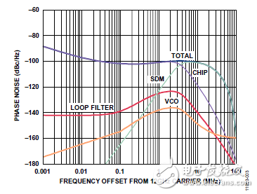
The maximum PFD frequency of the ADF4159 is 110 MHz. This means that the unfiltered SDM noise will peak at 55 MHz. Figure 3 shows the phase noise curve for a PFD frequency of 110 MHz. SDM noise occurs at a large offset from the carrier, so it can be filtered out using a loop filter.

Figure 3. Phase noise curve at 12 GHz output (fPFD = 110 MHz, LBW = 2.4 MHz)
The higher maximum PFD frequency of the ADF4159 is also important because it is recommended to keep the LBW below 1/10 PFD to ensure stability.
The ADF4159 has a maximum RF input frequency of 13 GHz. In this circuit configuration, the ADF4159 is actually driven by the VCO RFOUT/2 signal. This means that when the VCO mainly outputs 12 GHz, the ADF4159 is actually locked at 6 GHz.
This configuration means that a 24 GHz VCO can be used so that the 12 GHz RFOUT/2 signal is fed back to the ADF4159. The EV kit is sized to support a variety of 32-pin 5 mm &TImes; 5 mm LFCSP VCOs.
The ADF4159 internal charge pump has a supply voltage of 3.3 V. However, many wideband VCOs require a tuning voltage of up to 18 V. To meet this requirement, an active loop filter is required. The active filter multiplies the output tuning range of the ADF4159 by the gain of the op amp. See the AD8065 section of this circuit note for more details.
The ADF4159 supports programmable charge pump current characteristics. This feature allows the user to easily modify the dynamics of the loop filter without changing the physical components. At 2.5 mA charge pump current for this circuit, the LBW is designed for 2.4 MHz. The charge pump current can be reduced so that the LBW can be reduced without making physical changes to the loop filter components.
See the CN0302 Design Support Package for ADIsimPLL simulation of this circuit.
IP67 Waterproof HCF Power With Display
Ip67 Waterproof Hcf Power With Display,Display Power Converter,Led Power With Display,Outdoor Led Power With Display
Jiangmen Hua Chuang Electronic Co.,Ltd , https://www.jmhcpower.com