Interface technology with low electromagnetic interference, high throughput, low power consumption, and anti-noise interference will become an important part of the ultra-portable and consumer products market. This article will discuss some applications based on next-generation I/O technology that minimizes the risk of redesign, speeding up video baseband design and reducing electromagnetic interference (EMI) and overall cost.
This article refers to the address: http://
The mobile phone and portable device market in the Asia Pacific region (especially China) is the world's largest market. The focus of competition in these markets is not only the cost and performance of such products, but also the time they are put on the market. In China, local mobile phone suppliers account for more than half of the overall market. As Chinese handset manufacturers develop rapidly, they can quickly adopt new technologies such as radio frequency (RF) and baseband design in their designs. Engineers and end users are extremely savvy about technologies that can shorten design cycles, reduce costs and improve system performance. interest. Some applications based on next-generation I/O technology are discussed below.
Design challenge
1. High data throughput requires a new signaling solution
Since the resolution of high-end mobile LCD displays exceeds SVGA (800×600), the RGB data throughput between the application processor and the LCD module in the clamshell phone exceeds 750 Mbps (XGA mode, 60 Hz refresh rate). The existing transistor-transistor logic (TTL) technology's high swing (0V to VCC) between the baseband controller and the LCD module limits the signal data throughput between logic transitions, especially low electromagnetic interference requirements for edge rates. A limitation has been proposed. For TTL technologies with high data transfer rates, the low-bandwidth flexible cable between the flip cover of the mobile phone and the body may also increase the bit error rate, requiring the rework and redesign of the baseband, which can seriously delay the time to market.
In addition, because the next-generation camera phone has a resolution of more than three megapixels, RGB data throughput (read back to the baseband processor during snapshots) further pushes existing TTL technology to the limit. With all of these factors, the industry needs a new signaling solution to solve such problems.

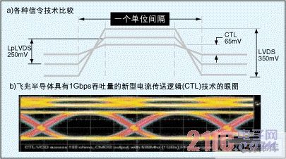
Figure 1: A brief comparison of various interface signal technologies and an eye diagram of CTL technology at 1Gbps speed
2. Electromagnetic interference and sensitivity
Low electromagnetic interference is almost a design challenge that is common to all handset designers. Due to the large amplitude, in order to quickly switch logic states, conventional TTL techniques typically have higher edge rates, causing reflection and electromagnetic interference problems. Reducing the edge rate of TTL signals, while reducing reflections and electromagnetic interference, limits data throughput. This problem is more pronounced in handset designs that use low bandwidth flexible cables to transmit signals. In order to achieve greater data throughput, the rate of edge change of the TTL logic must be increased, but this will also result in a higher rate of current change and will cause higher electromagnetic interference radiation over a larger frequency band. In addition, any reflection that occurs during logic level shifting not only causes more magnetic radiation but also increases the bit error rate. For mobile phone design, the electromagnetic interference around the flexible cable is very noisy, so it requires better common mode noise suppression, which is the characteristic of differential signal technology such as low voltage differential signaling (LVDS).
I/O solution
As noted above, low power, high throughput, and ultra-low electromagnetic interference signaling techniques are key to the design of portable and consumer product applications. Therefore, LVDS-like differential signaling technology has become an important design part of the system in terms of improving data throughput, noise immunity or electromagnetic interference performance. One of the biggest advantages of LVDS is its opposite current direction at the positive and negative outputs. If the positive and negative ends of the output are close enough, it should be able to cancel the electromagnetic radiation, which will greatly reduce the electromagnetic interference of the mobile phone and the impact on the communication signal of the mobile phone itself. Low-power LVDS technology versions (LpLVDS) with lower VCC capability are key to meeting portable design requirements in battery-powered applications such as cell phones that require lower power consumption. In addition to LpLVDS, Fairchild has developed next-generation I/O technology, Current Transfer Logic (CTL), to provide lower power consumption and lower electromagnetic interference.
Figure 1 shows a brief comparison of various interface signal technologies and an eye diagram of CTL technology at 1Gbps speed. Compared to traditional LVDS technology, CTL technology consumes 30% less power per channel. At the same time, CTLI/O's electromagnetic interference is 10dB lower than traditional LVDS technology and 20dB lower than TTL technology. The reason can be explained by using the waveform diagram in Figure 1. For the same time interval (which means the same throughput), CTL technology can easily be used between logic "0" and "1" using a much lower edge-rising rate. Switching, while the CTL swing is only 65mV, which is much smaller than the 350mV level of traditional LVDS technology. The lower di/dt is undoubtedly effective in reducing magnetic radiation.
Data transfer solution
LpLVDS and CTL only provide I/O solutions for interfaces between LCDs, camera imagers, and baseband processors. Both can only perform their powers when using some parallel-to-serial data transfer schemes. With phase-locked loop (PLL) technology, multiple parallel inputs can be converted to a serial stream using the multiplier frequency of the PLL output. This type of circuit is commonly referred to as a serializer. In the same way, when the data reaches the display side, the serial stream is decoded by the internal second PLL and converted back to the parallel TTL signal to drive the LCD module (LCM). The decoding circuit is called a deserializer. The dual PLL structure of the traditional serializer and deserializer increases power consumption. Fairchild's single PLLuSerDes can help designers save power and reduce power consumption with LpLVDS and CTLI/O. .

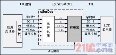
Figure 2: An application example of uSerDes in a smartphone design with an RGB interface.
Design example
Figure 2 shows the "write" operation of a typical LCD screen, where uSerDes based on LpLVDS or CTLI/O technology is used to pass RGB data from the baseband processor to the LCD display. This is a typical RGB interface in a dual-processor clamshell smartphone design. Using LpLVDS technology or CTL technology, the 16-bit TTL parallel data bus output from the LCD interface of the application processor is serialized into a single high-throughput differential data stream (D+ and D-). This design not only effectively reduces electromagnetic interference, but also significantly reduces the cost by eliminating a large number of cables and connectors between the body and the flip. In addition, because the electromagnetic interference radiation of LpLVDS and CTL technology is extremely low, there is no need to use an electromagnetic interference filter, which further reduces the cost.
Summary of this article
As the demand for multimedia applications such as high-resolution displays and cameras in 3G mobile phones grows, designers will gradually move from the current parallel TTL interface technology to differential serial interconnect technology. Interface technologies with low electromagnetic interference, high throughput, low power consumption, and noise immunity will become an important part of the ultra-portable and consumer products market, including mobile phones, camcorders, printers, and other pairs. A display terminal with limited power and electromagnetic interference.
Dot Matrix Led Display,Round Dot Matrix Led Display,5X7 Dot Matrix Led Display,1.2 Inch 5X7 Dot Matrix Display
Wuxi Ark Technology Electronic Co.,Ltd. , https://www.arkledcn.com