In the research and development of chips, FPGA verification is an important part of it. How to effectively utilize FPGA resources and pin assignment is also an important issue that must be considered. A generally better method is to allow the corresponding tools to be automatically allocated through some constraints of the timing in the synthesis process. However, it is often undesirable to consider this method from the development time period. The RTL verification and verification board design must be synchronized. The board that is verified when the verification code comes out must also be designed, that is, the assignment of the pins must be completed before the design code comes out. Therefore, the allocation of pins will be more dependent on people, not tools. At this time, it is more necessary to consider various factors.
Take into account the following aspects:
1. The signal flow of the logic carried by the FPGA.The FPGAs selected for IC verification generally have a very large logic capacity, and the number of external pins is quite rich. At this time, it is necessary to consider the difficulty of wiring during PCB design. If the pin assignment is unreasonable, then it is possible A large number of crossed signal lines appear in the PCB design, which brings great difficulties to the wiring, and even does not work, or even if the wiring is passed, it may not meet the timing requirements due to excessive external delay. . Therefore, before the pin assignment, the environment in which the FPGA works should be quite familiar. It is necessary to clearly identify where the signal comes from, and assign the corresponding signal to the nearest connection with the external device according to the shortest connection principle. In BANK.
2. Master the allocation of BANK inside the FPGA.The FPGA is now divided into several areas, each with a different number of I/O pins available. In the IC verification, the ALTERA and XILINX series FPGAs are used. The distribution of the internal BANK in the FPGAs of these two manufacturers is different, which can be consulted in the design. The following is an example of the allocation of the internal BANK of the FPGA in the StraTIx II series in ALTERA.

The figure details the allocation of BANKs inside the FPGA and the I/O standards supported in each BANK. According to the internal BANK allocation in the FPGA, combined with the flow direction of the signal in Figure 1, the direction of the FPGA in the board can be substantially fixed, and the relevant signals are allocated to the relevant BANK according to the nearest principle. The assignment of general signals can be done.
It can be seen from Figure 2 that the standard of I/O supported by each BANK in the FPGA is different, so the pins supporting the same standard should be concentrated into one BANK when the pins are allocated, because in the FPGA. The same BANK generally does not support two I/O standards at the same time. There are of course exceptions, which require reviewing the working conditions required by the relevant I/O standards.
4, pay attention to the assignment of pins for special signals The special signals here mainly refer to clock signals and reset signals, or some signals that require higher driving capability.
The clock signal is generally required to be assigned to the global clock pin, so that the time delay obtained will be the smallest and the driver will be the strongest. Since the reset signal has a strong ability to drive with good synchronization, it is normally fed from the global clock pin.
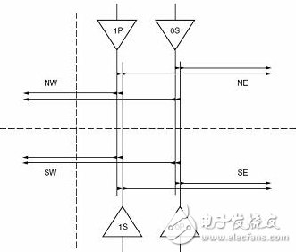
When allocating clocks, the strategies for assigning them according to the number of clocks are very different. They also need to be focused. This requires checking the corresponding manuals to see which clocks can reach which areas. The general clocks are differential clocks. If this is not used, Differential clocks need to be noted that the P and N terminals cannot be assigned to different clock signals at the same time. As shown in the figure below, if the paired clocks in the XILINX series of FPGAs are used at the same time, they cannot reach the same area at the same time because there is only one clock line that reaches the same area. So when the clock is low, it is best not to use P and S in pairs at the same time. Instead, just select P or N so that there is no conflict.

5, taking into account the consideration of signal integrity.
Since bus allocation often occurs in the allocation, and a large number of buses may often be flipped at the same time, this will bring a series of signal integrity problems, so a large number of simultaneously flipped signals in the pin assignment separate.
Open Frame For Infrared Touch Monitor
GreenTouch's LCD open frame for infrared Touch Monitor is a touch solution developed for automated information systems, gaming and entertainment, as well as light industrial automation controls,making GreenTouch's touch monitor product line even more complete.The touch monitor display is based on the concept "Design for simple and convenience", with proven GreenTouch expertise and reliability.GreenTouch's open frame touch monitor delivers an perfect solution that is cost-effective for worldwide customers requiring a reliable product .Designed with reliability from the start, GreenTouch's open frames deliver outstanding image clarity and light transmission with stable, drift-free operation for accurate touch responses.
* Display Type: Active Matrix TFT LCD, LED Backlight
* Touch Type:Infrared ,10 Points Touch
* Display Ports:VGA+DVI,VGA+DVI+HDMI,VGA + DVI + HDMI + DP
* Touch Systems:Windows,Android,Linux
* Certificates:UL,FCC,CE,CB,HDMI
* Warranty:1 Year
* Customized:Support


Dust-Proof Industrial Touch Monitor,Waterproof Industrial Touch Monitor,Anti-Interference Touch Monitor,Wall-Mounted Embedded Touch Monitor,Infrared Touchscreen Monitors
ShenZhen GreenTouch Technology Co.,Ltd , https://www.bbstouch.com